Journal CSS

The Journal of The Institute of Circuit Technology Vol 14 No 2 August 2021 |
|
| Links to Contents | Section |
| 5 | |
| 7 | |
|
Industry News: Macdermid Alpha, CC Electronics, Eurotech, Merlin PCB |
|
|
Members News: Maurice Hubert, Foundation Course Attendees, Exception PCB- Lisa Trust |
|
|
Section 1 |
Editors Introduction It's a Material World |
|
Lynn Houghton Journal Editor |
In this journal we bring you material developments from Isola and Circuit Foil for High Speed and Automotive EV applications. Mark Goodwin calls for closer designer-supplier cooperation to ensure optimum material selection in this "performance hungry world". |

|
Section 2 |
Editorial Recover to the New Normal Paul Goodfellow, Minnitron Ltd, Ramsgate, UK |
|
|
Irrespective of your industry, your vocation or even your country it seems that our lives will be different from this day forward! Many factors need to be addressed on a daily basis and some of the following questions may be relevant…… How resilient is our supply chain? It is more important than ever that companies seek out change. We can make changes to a number of key areas and I have used our experience at Minnitron as an example.. We are holding more stock of more difficult to source materials. We are also looking even more closely at training for the already highly skilled and experienced staff as the investment in every individual pays huge dividends in product quality, consistency and of course the bottom line! I can never understand businesses that continually invest in their people but are unable to retain them! Staff and training thereof are huge costs and there is no point in training alone. If they aren’t happy for whatever reason, they simply won’t stay and then it is all a waste. Minnitron Ltd has seen a lot of ups and downs in our 58 years of PCB manufacture. None quite like the COVID -19 pandemic but we have a proven track record in evolving through difficult times. I am happy to share these thoughts with you. We should all explore the opportunity in the chaos and make the best of this difficult time to once again thrive in moving forward. |
 Paul Goodfellow
|
Section 3 |
Calendar of Events |
|
Date |
2021 Events |
|
25th February 6th April - 27th May 1st June 7th September November |
AGM Webinar / Zoom Meeting Webinar Foundation Course Lectures Annual Symposium Webinar Autumn Webinar Evening Seminar and Facility Tour - Date to be confirmed |
|
|
|
Section 4 |
New PCB material for demanding high temperature and high voltage requirements of the rapidly growing automotive EV market Anna Graf and Michael J Gay, Isola Group |
|
Michael J. Gay
|
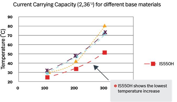
With the rise of automotive electrification, electronics system designers face significant challenges to achieve long-term, high reliability. The need for high voltage operation and fast charging coupled with reduced pitch and conductor spacing (miniaturization) requires the use of a material to enable designs for these extreme conditions. PCB’s will require a base material that has the capability to withstand electrochemical migration while operating in harsh environments at high voltage loads and extreme high temperatures. In order to meet these major challenges Isola has developed a new material based on a unique resin technology. IS550H prepregs and laminates are glass reinforced, halogen free benzoxazine resin system materials, that still offer FR-4 processability combined with a thermal stability that go beyond an FR-4 High-Tg epoxy resin system and extreme CAF resistivity. For electronic devices used in the electric power train of e-cars, for example, inverters and converters, where the requirements regarding thermal stability and high voltage CAF resistance are increasing. Operating temperatures up to 150°C are already requested. This may rise even up to 175°C when the new generation of semiconductors, like SiC, comes to use. These wide bandgap semiconductor materials will enable increased driving ranges and faster charging times. So the interest is high in the industry to push this technology. As operating temperatures up to 175°C are very challenging for FR-4 epoxy materials currently ceramics are options to meet this challenge. The main disadvantages of ceramics are the non-standard processability and high cost. That´s why Isola developed IS550H on basis of a benzoxazine resin to offer an organic, cost effective alternative to ceramics for these requirements to the market. 800V technology devices are already used in electric cars series production. Base materials used within this technology have to prove their high voltage CAF resistance up to 1000 V. With regards to the rapidly developing market also voltage ranges beyond 1000 V are considered. Beside temperatures and voltages the operating time also becomes a critical factor. With a combustion engine vehicle the operation time is equal to the driving time. With an e-car the operation time is not only driving time but also charging time. This means that required testing cycles and hours have doubled or even tripled depending on the acceleration factor and test used. The standard 1000 cycles and 1000 hrs are no longer sufficient. 2000 cycles in TCT and up to 3000 hrs duration time in high voltage CAF test are today’s requirements. IS550H has been extensively tested in regards of its suitability for all these demanding requirements. It passed 2000 hrs storage testing at 175°C with embedded copper coin TV´s and can be used for peak temperatures up to 200°C. It has shown an extremely high reliability and crack resistance when tested in thermal cycling test -40°C to 175°C for 2000 cycles. Beside these extreme thermal stability properties, it also has a significant improvement over FR-4 type materials with a thermal conductivity of 0.70 W/mK that enables embedded heat sink applications and an effective heat distribution within the material while heat losses are induced during operation. (Fig1)
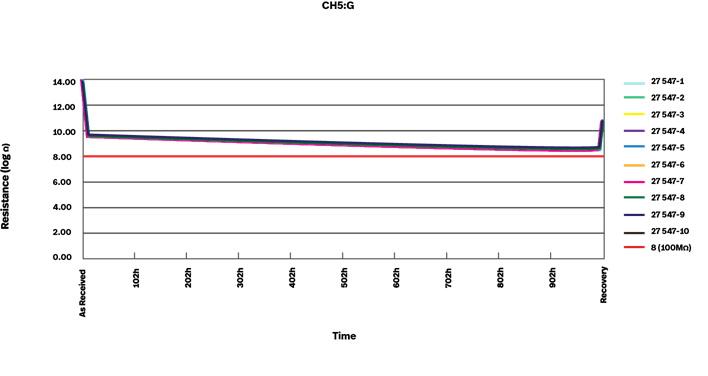
Fig 1: Current Carrying Capacity test with 100 A, 200 A and 300 A performed on TV produced with IS550H and three other high Tg base materials IS550H has demonstrated furthermore to achieve CAF performance at 1500V for 1000 hours for tight pitch, PTH to PTH and z-axis structures. (Fig 2 & 3) While it is not FR-4 material, IS550H’s processability is easy like common filled FR-4 materials.
Fig 2: 1000 V, 85 °C, 85 %RH, 1000 h CAF test; HW-HW distance 0.85 mm
Fig 3: 1500 V, 85 °C, 85 %RH, 1000 h CAF test; HW-HW distance 1.05 mm Although IS550H was developed targeting electric vehicle applications, its extreme thermal stability makes it of course suitable for all thermally challenging devices like ie downhole drilling, avionics / military or engine management. Until now devices where thermal stability and reliability requirements go beyond epoxy FR-4 materials capability were realized with Polyimide base materials. With IS550H there is an excellent possibility to offer a material which can be used at higher temperatures compared to FR-4 and fills the properties gap to the Polyimide materials. IS550H is available with core thicknesses ranging from 0.0020 inch (0.05 mm) to 0.063 inch (1.5 mm) and a wide range of prepreg resin contents for most applications including heavy copper designs. Please visit our website at www.isola-group.com for more information. |
| Go back to Contents |
 Anna Graf
|
Section 5 |
Choosing the Right Materials is Tougher Than Ever Mark Goodwin, Ventec International Group |
 Mark Goodwin Mark GoodwinChief Operating Officer, Ventec International Group |
The combination of rising performance expectations, intense commercial pressures and unexpected supply chain disruption means that choosing and getting hold of the right substrate materials for product designs is tougher today than it has ever been. As a wider selection of materials, with more finely nuanced properties, becomes available to designers, making the right choice is also increasingly complicated. Fortunately, help is available from suppliers and industry bodies. But designers can also help themselves by being more willing to share information with their suppliers. Calling for closer working partnerships may be going against the grain in times of the global pandemic, as social distancing practices look set to continue to be an integral part of our daily lives. However, it is vital for us all to be more open from a technical standpoint if the next generations of high-tech products are to meet the world’s future needs. Complex, performance-hungry technologies like 5G and AI simply must succeed if we are to have the foundations necessary for smart living: smart energy, smart cities, smart buildings, smart factories, and smart healthcare are essential to ensure a high quality of life for all while preserving the planet’s resources. As PCB industry veterans, we are well aware that the board is typically the last part of the project to be specified when a new product is being designed. On the other hand, it’s the first item to be needed when serious development begins. Designing the circuitry to go on the PCB obviously gets most of the attention, but the substrate itself is usually the lowest priority in engineers’ minds. When the time finally comes to consider it, teams will often simply default to using the same materials as were used previously. As the performance demands imposed on successive product generations continue to intensify, and factors such as conductive anodic filament (CAF) formation that seriously affect reliability become more critical, this approach is increasingly unsatisfactory. As the industry has come to understand more about how the substrate properties influence performance and reliability under various operating conditions, so the number and diversity of material types on offer has increased. In the past there have been only a handful of options open to designers. Today, international specifications offer over 100 different material categories to choose from. Designers, understandably, struggle to connect the specifications with the properties they are looking for. It doesn’t help that these specifications are usually based on chemical composition. As the breadth of choice on offer continues to increase, it’s almost impossible for electronics engineers to relate to them. At Ventec, we have been calling for some time for the industry to move to performance-centric specifications that are easier for engineering communities to interpret. Getting help is essential, because struggling on alone risks under-specifying or over-specifying the material for the application at hand. Neither is good: under-specifying risks the product coming up short in a way that could be beyond any realistic remedy. Over-specifying, to be “on the safe side”, can be commercially disastrous in ultra-competitive markets such as consumer technology. The chosen materials also need to be readily available in any location globally where the product is to be manufactured. Some resins, for example, are only available in certain domestic markets and are difficult to procure elsewhere. So, what’s the solution? Qualifying or testing materials helps to understand their performance and properties but is expensive and time consuming for companies to undertake independently. Pooled testing, where groups of companies get together to do specific tests and share the results, is one response. There are a variety of industry initiatives that benefit from pan-industry participation that offer comprehensive sets of analyses that cover things like Dk and Df, CAF, thermal stress, and other tests on standardized test coupons. Designers can also take advantage of another emerging trend among suppliers, which is to present carefully curated sets of materials for specific application areas. Our autolam and aerolam material guides (aerolam is launching this year), for example, bring together products with properties suitable for automotive or aerospace and further sub-divide them according to target applications and operating environments, such as under-the-hood or in-cabin. In this way, companies like Ventec effectively contribute their expertise to help customers shortlist products that can meet their requirements. This helps by simplifying and accelerating selection, narrowing the focus onto materials that are fundamentally suitable. Helpful though this is, as suppliers we often need designers to express their requirements directly if we are to provide the right material for the right task. It’s of course understandable for any OEM to be wary of sharing information about their intellectual property and product strategies, but the value of trust between OEMs and their supply partners cannot be underestimated. As the issue of materials selection becomes more complex and, at the same time more important to get right first time, there is increasingly more to gain by finding ways to be open and more to lose by keeping traditional barriers in place. |
| Go back to Contents |
|
Section 6 |
Ultra Low Profile Copper Foil for Very Low Loss Material Thomas Devahif, Circuit Foil, Luxembourg |
|
|
ABSTRACT Copper foil roughness has become a significant factor influencing conductor loss in high speed PCBs, particularly as they move above the 50 GHz range. At high frequencies, the current tends to flow mostly on the surface of the conductor (skin effect). When the so-called skin depth reaches the same dimensions as the roughness profile of the foil, the current follow its contour, inducing additional loss due to the longer propagation path. For regular very low profile copper foil, the roughness is around 3.0 µm (Rz ISO), meaning that the loss becomes significant at frequencies close to 1 GHz. To achieve good results over 50 GHz, the profile roughness must be well below 1.0 µm. New ultra-low profile copper foils have been developed to achieve this property while maintaining a good adhesion with very low loss resins. Electrodeposited copper foil production is divided in two steps. First, the foil is plated on a titanium drum from a copper sulphate solution. Then a treatment is applied to increase roughness and ensure oxidation resistance. By using organic additives in the plating bath, the structure of the product can be controlled and the roughness decreased. Further improvement was achieved with titanium drums that had been polished with a specific grinding wheel to achieve a lower roughness on their surface. With a combination of both improvements, copper foils with roughness below 0.7 µm have been obtained. The adhesion is usually increased with the treatment step by applying nodular copper particles. However, regular treatments have a significant impact on the roughness and therefore on the signal loss. A good compromise between adhesion and transmission properties was achieved with specific nodular deposits. For ultra-low loss application, a version of the foil without treatment has also been developed. Sufficient adhesion is ensured by silane-based coupling agent or organic coating. Key words: INTRODUCTION When an alternating current is going through a conductor, the changing magnetic fields induce the formation of additional electric fields (Eddy’s currents). Those fields are opposed to the “main” current in the centre of the conductor, but strengthen it on the outside (Figure 1.), resulting in an increased current density on the surface.
This phenomenon, called skin effect, is stronger with higher frequencies. The effective section of the conductor where most of the current flows (the so-called skin depth) can be estimated with the equation below: Where δ is the skin depth (m), f the frequency (Hz), µ the magnetic permeability (H.m-1) and σ the electrical conductivity (S.m-1) of the material (copper). The skin depth is a measure of the distance from the surface of the conductor at which the current density falls to 1/e of its value on the surface [4]. Around 98% of the current flow at distance of four times the skin depth. It is below the micrometre range for frequencies over 4 GHz (Table 1.).
Skin effect has two impacts on the conductor loss. Firstly, the effective cross-section of the conductor carrying the current is reduced, inducing a higher AC resistance. Secondly, for conductors with a rough profile, a low skin depth will cause the current to follow the contour of the material, increasing the effective length of the propagation path (Figure 2.). It has been demonstrated that surface roughness can double the conductor loss [5].
To mitigate this effect, copper foil manufacturers must develop new profile-free products. For regular copper foils, the roughness is voluntarily increased to improve the adhesion. It is considered that over 90% of the peel strength between a rough copper foil and a prepreg is due to mechanical forces, while the remaining peel strength is due to chemical adhesion. On a low or no-profile copper foil, the mechanical strength is drastically reduced. IPC-4562 defines 3 major classes for roughness profiles, irrespective of the foil’s thickness (Figure 3.). Below 5.1 µm (200 µinch) is defined as “very low profile”. However, this definition is behind the industrial progress. Latest low roughness copper foils are usually named as “HVLP” (Hyper Very Low Profile Copper), with incremental numbers for each new generation. HVLP would have a roughness below 3.0 µm Rz ISO, HVLP2-3 below 1.3 µm and HVLP4-5 below 0.9 µm. The distinction between HVLP 2/3 and 4/5 is related to the type of treatment applied, not so much impacting Rz values but rather more accurate parameters such as 3D measured surface developed ratio. Another gap is found among definitions of Rz since Rz ISO is not identical to Rz JIS. For very low roughness, this difference is significant and can be above 25%.
This paper discusses the development of HVLP 2 to 5 copper foils with a roughness below 1.0 µm in Rz JIS, i.e. 1.3 µm (50 µm inch) in Rz ISO (all the roughness data presented below are expressed in Rz ISO). Electrodeposited copper foil manufacturing The second step of copper foil manufacturing is the treatment. Several electro-chemical processes improve the foil adhesion and ensure oxidation resistance. Firstly, copper nodules are deposited on the foil to increase its surface area and therefore the adhesion. To obtain this, specific electrolysis conditions must be used: low copper concentration with high current density (Figure 4.).
Roughness Measurement
Background
The roughness of foils produced only with levellers falls into the range of “low profile” product (4-6 µm for 35 µm (1 oz./ft²) thick foil). HVLP foils are produced by combining levellers and other types of organic additives called brightners that can give the electrolyte side of the foil a smooth and shiny aspect (Figure 6.). The roughness of those HVLP foils is around 1.9 µm (Table 3.).
Production of ultra low profile foils
.
With a specific preparation method, the drum surface roughness could be decreased down to 1.25 µm. The impact on electrolyte side roughness is estimated to be in the 0.1 to 0.2 µm range. Long term production runs have highlighted that the polishing done after each roll to remove the oxidation on the drum’s titanium surface had little to no impact on its roughness (Figure 8.).
With both additives and drum surface improvements, the roughness could be decreased well below 1.0 µm for all thicknesses (9, 12, 18 and 35 µm). Those improvements are reflected in the insertion loss measurements (Table 5.). HVLP3 and 4 foils have significantly improved electrical performances compared to first generation HVLP. From a mechanical point of view, ultra-low profile foils behave like any regular low profile copper foil.
TREATMENT OF ULTRA LOW PROFILE COPPER FOIL
Low profile nodular treatment applied on HVLP foils is a uniform layer of round-shaped nodules covering the surface (Figure 9.). With a nodule size around one micron, it ensure excellent adhesion and thermal resistance at the expense of a significant increase of roughness compared to the base foil (+ 0.5-0.7 µm of Rz ISO). HVLP2 benefits from a lower roughness base foil, but also a treatment with a 5 fold nodule size decrease compared to HVLP. It offers a good compromise between adhesion and electrical performances.
As further decrease of treatment size would result in insufficient peel strength, a different methodology was followed for HVLP3 foil. In this case, the use of specific silane based adhesion promoters in combination with appropriate surface finish greatly increased the contribution of chemical adhesion, allowing further treatment size reduction (20 times smaller than HVLP2). For HVLP 3 or 4 type foil, we estimate that mechanical adhesion accounts for only 50 % of total adhesion, instead of more than 90 % for previous generations copper foils. Interestingly, when comparing HVLP 3 and 4 whose only difference is the base foil roughness, HVLP4 tends to have higher peel strength. It is assumed that the smoother surface allows for a more homogenous treatment deposition, improving its properties. On HVLP5, the fine tuning of passivation chemistry and the use of high adhesion silane coupling agent allowed to reach good peel strength on most low loss materials with a nodular free copper foil. However, silane type may have to be changed depending on the targeted resin system in order to ensure optimal adhesion.
Passivation ROUGHNESS MEASUREMENT
A more appropriate surface roughness measurement for ultra-low profile foils is the white-light scanning interferometry. The principle is to divide a light beam in two paths, directing one to a reference mirror and the other one to the sample surface. This measurement beam travel different distances depending on the surface profile. The two waveforms are then recombined and create interference patterns depending on their phase difference. Those patterns are analysed to calculate the height of the sample at each point (pixel) scanned [10]. Unlike the stylus method, light interferometry does not damage the sample and can measure height differences smaller than 0.1 µm. 3D roughness are expressed as “S” parameters such as Sa or Sz. Depending on the parameter, different information about the surface profile will be available. For example, Sz value which is the height difference between higher an lowest point on the surface is much less sensitive to the treatment size as it is usually smaller than the roughness range (waviness) of the base foil. It can be correlated to some extent with the Rz measured with a profilometer. Sa which is the arithmetic mean deviation won’t be greatly impacted by latest generation treatment (HVLP3/4) either. The sdr – defined as the ratio between the developed surface and a perfectly flat one having the same dimension – is however very sensitive to the nodular treatment size and surface area, parameters which are critical for insertion loss properties. Therefore, we consider Rz, Sz and Sa to be macroroughness parameters more related to base foil roughness for ultra-low profile copper foils, while sdr is a microroughness measurement.
CONCLUSION The use of white-light scanning interferometry ensured an accurate measurement of the foil’s roughness, even for the smallest treatment features.
FUTURE WORK
REFERENCES |
| Go back to Contents |
 Thomas Devahif
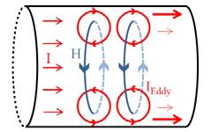
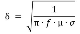
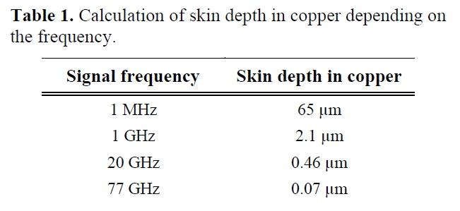
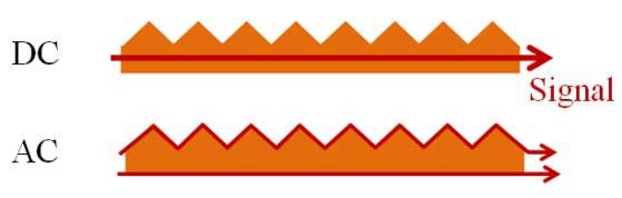
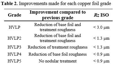
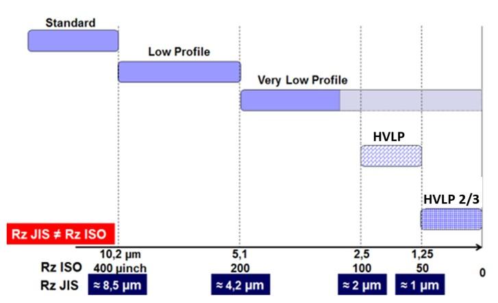 Figure 3. Grades of copper foils roughness [6]
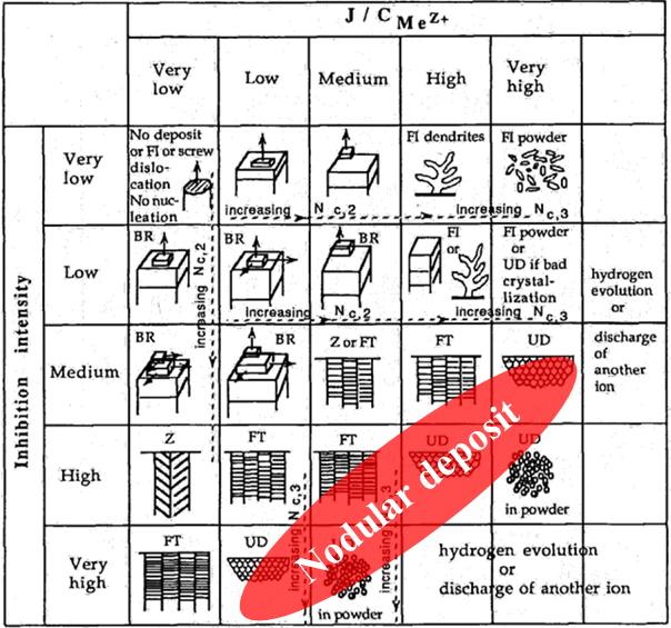 Figure 4. Copper deposit structure depending on electrolysis parameters
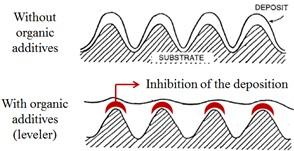 Figure 5. Copper deposition with and without organic additives (levellers) [8].
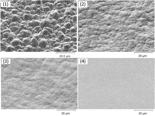 Figure 6. SEM imaging of 35µm (1 oz./ft²) base copper foil prior treatment:
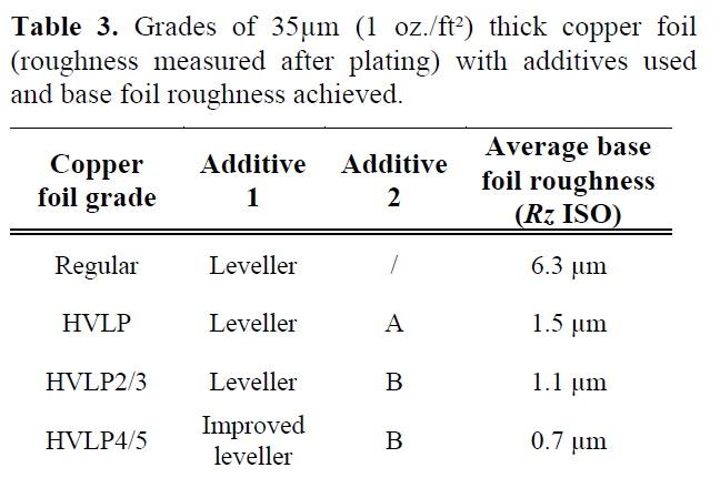
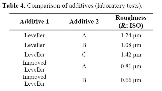
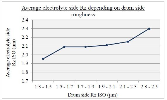 Figure 7. Impact of drum side roughness on electrolyte side
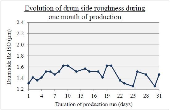 Figure 8. Evolution of drum side Rz during one month of production
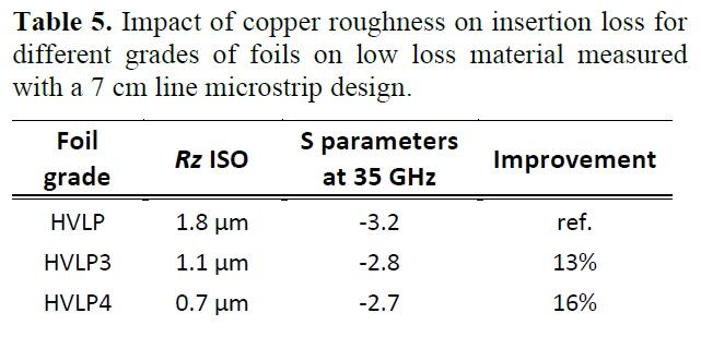
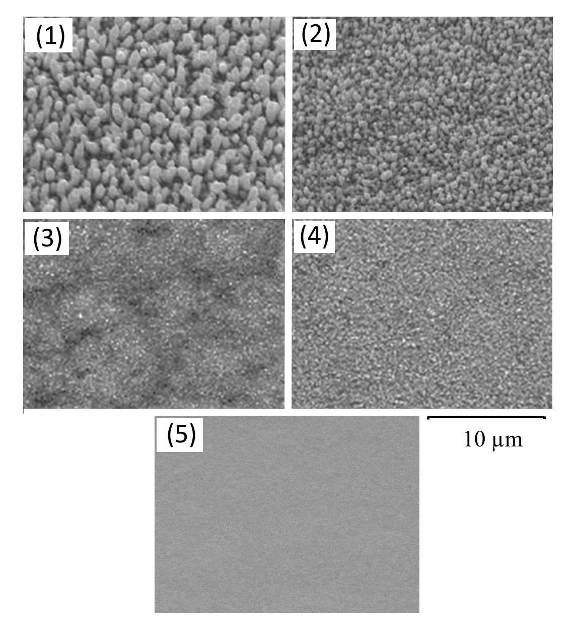 Figure 9. SEM pictures of (1) HVLP, (2) HVLP2, (3) HVLP3,
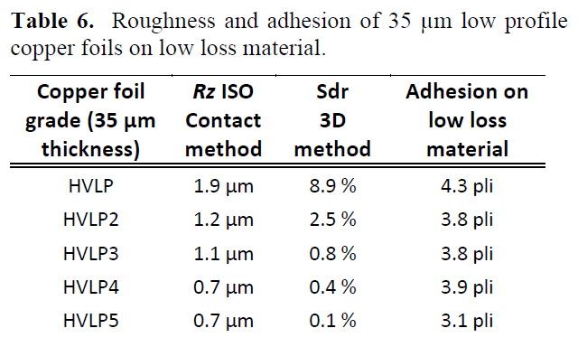
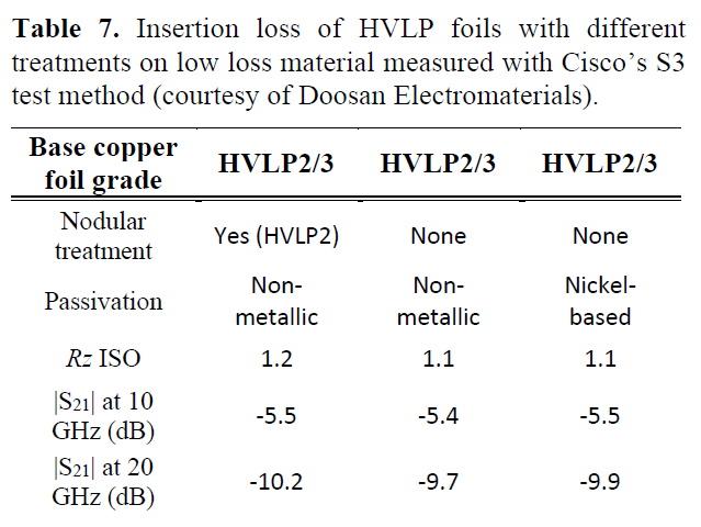
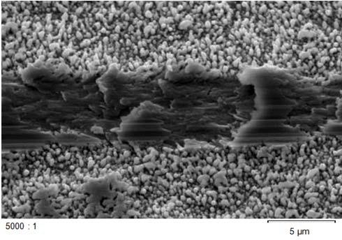 Figure 10. SEM picture of the trace left by the stylus used
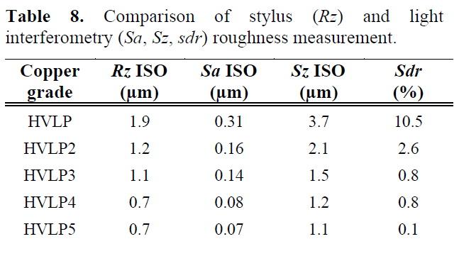
|
Section 7 |
ICT Webinar Review June 1st 2021 Recyclable PCBs, and More Pete Starkey, I-Connect007 |
 |
Another excellent technical webinar on June 1, introduced and moderated by ICT Chair Emma Hudson, provided updates on developments in recyclable PCBs, innovations in transparent flexible displays, and X-ray fluorescence techniques for the determination of the thickness and composition of metal coatings. “It is time for us to take responsibility for our electronics and the impacts that they are having on the planet,” said Jack Herring, CEO of Jiva Materials, who reported the progress of the ReCollect project for recyclable PCBs. |
 |
Recyclable PCBs Commenting that 32% of all e-waste consisted of small domestic equipment and that current recycling techniques for the recovery of precious metals such as gold, silver, and palladium involved shredding and incineration, he explained that the focus of the ReCollect (Recyclable Composite Laminates for Electrical Goods) project was to develop an alternative way of managing end-of-life circuit boards by removing difficult-to-recycle fibreglass-epoxy PCBs from the supply chain. Primary objective was to demonstrate the feasibility of producing a PCB substrate in high volumes within the UK, with performance comparable to CEM1 and FR-4, with circuits formed by additive or subtractive techniques. An important secondary objective was to ensure its compatibility with existing aqueous fabrication processes. Target market was the white goods and domestic appliance sector, including dishwashers, fridges, and washing machines, the manufacturers of which already had well-established recovery schemes in place, enabling PCBs made on the new substrate to be removed and recycled. Jiva’s patented solution was a flame-retardant composite of natural fibres and a polymer resin that dissolved in hot water yielding non-toxic and biodegradable by-products, avoiding energy-intensive recycling by shredding and incineration and enabling substantially higher yields in precious metal recovery. Herring estimated the soluble PCB to have 60% lower carbon footprint than the equivalent FR-4 product and a plastic saving equivalent to 620 grams per square metre. Indeed, if used in just 1% of European domestic appliances, 100 tons of plastic could be eradicated. Small quantities of PCBs had been produced in Jiva’s UK development laboratory and the recycling process was being developed to establish a take-back scheme for end-of-life electronics and enable customers to benefit from an effectively circular supply chain. Herring showed examples of single- and double-sided printed electronics on unclad substrate, assembled using conductive silver epoxy, with low-temperature soldering in development. Copper-clad laminates had been manufactured, and mechanical drilling and routing parameters had been established. Etching had been successfully demonstrated and processes for through-hole connectivity were being explored. The substrate was thermoplastic and potentially mouldable into three-dimensional profiles. An extensive third-party testing programme was nearing completion, and had shown mechanical properties to be comparable to CEM1 and electrical properties comparable to CEM1 and FR-4. Flame retardancy was in line with UL 94 V-0, and it was planned to submit samples for formal UL classification in Q4 2021. The material had attracted interest from white-goods, LED lighting, and computer-peripherals industries. |
 |
Transparent Flexible Lighting The topic of the second presentation was developments and innovations in transparent flexible lighting, delivered by Dr. David Shaw, business manager for semiconductor technologies at A-Gas Electronic Materials. He explained that although indium tin oxide had become established as the industry standard transparent conductive film and would continue to be dominant on glass substrates, it had limited capability for flexible applications. It was not formable or stretchable, it was not as transparent or as conductive on plastic as on glass, and circuit patterns were costly to create. Alternative materials included conductive polymers such as PEDOT, silver nanowires, and copper or graphene micromeshes, none of which could fully satisfy the combined needs for transparency, conductivity, affordability, environmental stability, flexibility and formability. A carbon nanotube—silver nanowire hybrid material had now been developed which not only met these requirements but could also be cost-effectively patterned by basic technologies without the need for high-resolution laser ablation. A flexible film, roll-to-roll coated with a silver nanowire dispersion, was screen-printed with a conductor pattern using a carbon nanotube ink, after which the exposed silver nanowire areas were removed with a mild ferric nitrate etchant to create a patterned transparent conductive film. A range of sheet resistances from 10 to 75 ohms per square could be achieved. If copper micromesh materials were used, sheet resistance could be reduced to 1 ohm per square. Application areas included transparent heaters, transparent antennas, transparent lighting films and transparent touch sensors, and there were enormous growth opportunities in automotive, transparent LED and digital signage market segments. |
 |
X-ray Fluorescence Techniques With the proliferation of thin metallic final finishes for soldering and wire bonding: ENIG, ENEPIG, EPAG, RAIG, IGEPIG, DIG, and so on, accurate thickness measurement has always been a challenge. It must be fast, precise, non-destructive and cost effective. The IPC-4552A performance specification for ENIG refers to X-ray fluorescence methods, making some recommendations regarding instrumentation, discussing verification of the measurement process and assessing its capability. In the final presentation, Zach Dismukes, global product manager with Bowman Analytics, reviewed new developments in X-ray fluorescence techniques to enhance throughput and precision in ENIG and ENEPIG measurement. He began with an enlightening introduction to the principles of X-ray fluorescence, without venturing too deeply into the theoretical physics, describing how X-rays interacted with inner-shell electrons to cause some to be ejected and be replaced by electrons from higher orbitals, filling the holes left behind. The energy difference of electrons moving between orbitals was released in the form of photons with a specific wavelength characteristic of the element. Thus X-ray fluorescence related to the absorption of radiation of a specific energy, resulting in the re-emission of radiation of a different energy. This gave the basis of a spectroscopic analytical method for measuring elemental composition and plating thickness. In principle, the method was applicable to all metallic elements from aluminium to uranium, at thicknesses from sub-nanometre to microns, and could measure thickness and composition simultaneously, up to five layers and 25 elements. Recent developments in X-ray fluorescence spectroscopy gave improved stability and enabled the statistical capability requirements of IPC-4552A to be met with a shorter measurement time. Dismukes explained the advantages of large-window silicon drift detector technology, and polycapillary optics for optimised focusing of x-ray beams. He also discussed the characteristics of different tube targets and described some of the advanced software-automation features now available, such as autofocus, pattern recognition, XYZ programming, and fully-customisable data-export for automatic generation of reports. |
 |
After moderating a Q&A session, Emma Hudson thanked all participants and particularly acknowledged ICT technical director Bill Wilkie’s smooth organisation of the event. Although ICT’s series of technical webinars had been extremely successful, she was hopeful that there could soon be a return to live seminars and symposia with all of their networking benefits. Published by kind permission of Pete Starkey, I-Connect007 The Webinar can be viewed on the ICT You Tube Channel here |
|
Section 8 Foundation Course |
Annual Foundation Course 2021Bill Wilkie, ICT |
|
Bill Wilkie |
This year’s Annual Foundation Course has been unlike anything in it’s history, starting in 1980 in Galashiels College of Further Education. Moving swiftly to Heriot Watt campus and then through Loughborough University and eventually Chester University, it began as a two week residential course and transformed with the PCB Industry into a tight course over four and a half days. The first day was sponsored by Merlin at their Deeside plant so we could take in a facility tour, a staple part of the event going right back to the start of the course With the UK’s universities closed to all events due to covid, an idea was born and began to emerge last Autumn. Lecturers were sounded out and a schedule put in place for Tuesdays and Thursdays every week during April and May. Member companies who had sent delegates in the past were canvassed and then we distributed the idea in a mail shot to all our members. We had a crash course in meeting platforms in the Autumn and signed up for Zoom – no going back. Thanks also to the following who attended the lecture hours, which were job specific. Amphenol-Invotec Holders Technology Sun Chemicals |
| Go back to Contents |
|
Section 9 |
PCB Fabricators Group - a Benefit to all who Fabricate PCB’s in the UK. |
|
Matthew Beadel |
The fabricators group met for its 2nd meeting of 2021 and again the turnout was high – a trend that we hope will continue for the future. The meeting was ‘as ever’ very interesting and again lasted the 2 hours as there was plenty to discuss. Some of the topics of discussion centred around both Covid (mainly restrictions of service engineers from Europe and USA) and the aftermath of Brexit (which is still being felt). The group as a whole believed that the UK PCB industry was ‘heading in the right direction’ even though there’s been many bumps in the road. There was however concerns over supply of laminate and the various increases in material cost and very extended leadtimes that have been imposed on the Fabricators by many (although not all) suppliers. Copper foil supply was also discussed as a potential issue with the increase in requirement for Electric cars, although not something that has been felt too severely in the UK yet – the following months will be telling! As always we are very happy to welcome new members to the group, please let either Bill Wilkie know or contact the Fabricators group directly. |
|
Section 10 |
Industry News |
||||
| Company |
Title |
||||
| Macdermid-Alpha |
King's Day Converting a long running, one-week Annual Course into a 16-week lecture series was never going to be without problems. We were able to resolve issues of missing emails, quantify the struggle with bandwidth and broadband speeds, but when it came to last minute replacements for lecturers, we were almost stumped. It was at the eleventh hour that we managed to track down a MacDermid Alpha representative from the Netherlands, called Hans Vrijhof, who mailed that he might be able to do something similar to the ‘Etching and pre-treatment’ Lecture. He subsequently gave me a call and I discovered that this stalwart was actually on a public holiday, called King’s Day and would have to forswear all drink until he completed the presentation. I quickly found out that the King’s Day celebration is held every year on the 27th April, with revellers dressing in orange costumes and generally having a good time.
The Royal Family on Koningsdag Our thanks to Hans Vrijhof of MacDermid Alpha for stepping in at the last minute and also supplying these pictures of King’s Day. |
||||
| CC Electronics |
UL Approval for Halogen Free Laminate CC Electronics is proud to have been approved for Halogen Free laminate. If you have any feedback or questions about Halogen Free Laminates or would like to request a quote Simply get in touch by emailing |
||||
| Eurotech |
Alan Green, GM at Lyncolec: 54 Years In The Making! Lyncolec Ltd. are quietly celebrating something quite monumental. Alan Green is our General Manager and he is celebrating 54 YEARS cumulative experience in the Printed Circuit Board (PCB) industry! Alan has worked with many prestigious PCB manufacturers since 1967, and has witnessed first-hand the evolution of the industry and products which accompany it. Let's put that into context...Read more... |
||||
| Merlin PCB |
Merlin Circuit Technology Ltd Laser Drilling and Stacked Via Technology Merlin has recently increased its technical capability with the introduction of laser drilling and stacked via processes. This has been achieved with the financial assistance of SMART CYMRU and the European Regional development fund. This technology complements the other high technology processes already being offered by Merlin Circuit Technology at its facility in North Wales. Read more.... |
||||
| Go back to Contents |


| Section 11 |
Members News |
|||||||||||||||
|
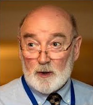
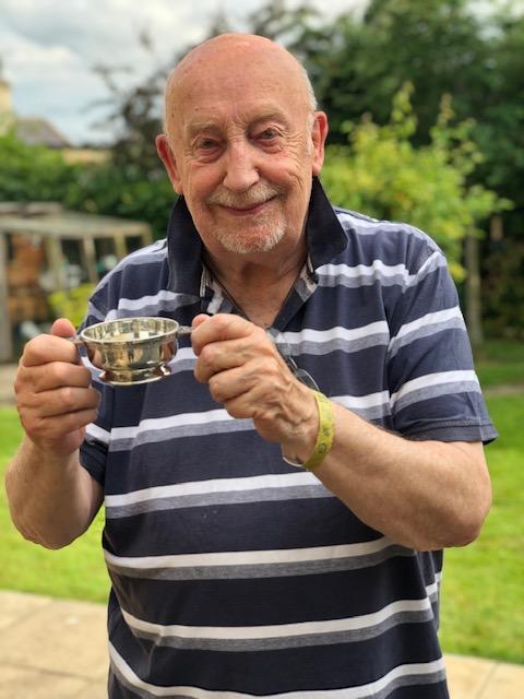
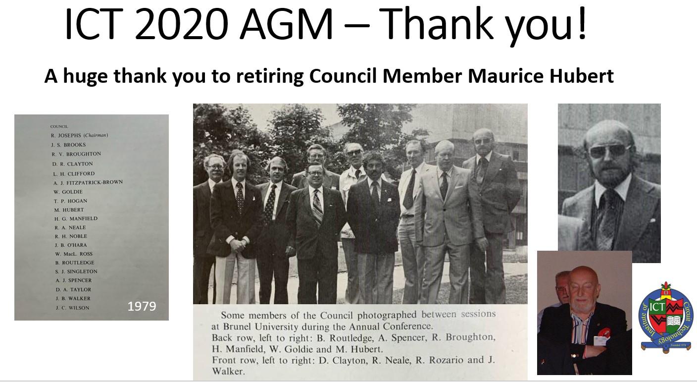
Maurice Hubert
|
|
|||||||||||||||
| Foundation Course |
Some of the Succesful Participants of the Foundation Course 2021
|
|||||||||||||||
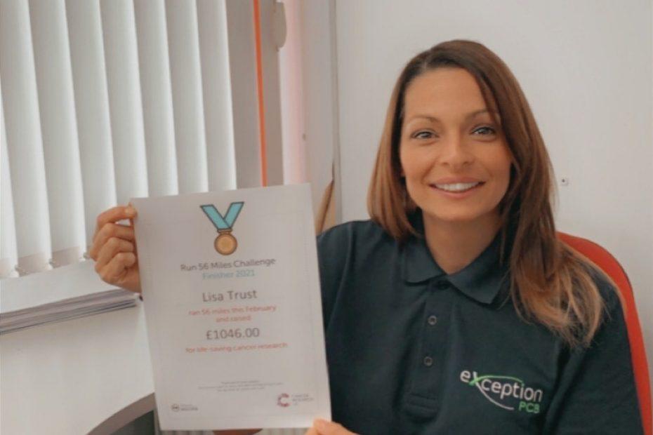
| Exception PCB |
Lisa Trust, Production Control, raises over £1000 for Cancer Research UK
With lockdown in 2020, being furloughed and COVID hitting everyone’s mental state of mind I needed something to give me a boost. After Christmas a challenge to run 56 miles in February 2021 for Cancer Research, popped up on Facebook. This seemed like the perfect way to clear my head and help out a great charity, I hadn’t run for almost 2 years due to various injuries so it was always going to be a challenge not only the finish 56 miles but to not pick up another injury. A group of us at Exception have completed a few charity walks, we did the 3 peaks for Birmingham Children Hospital in 2018 and 5 Valleys Walk in 2019 for Meningitis.
|
|||||||||||||||
| Go back to Contents |


|
Section 12 |
Membership News |
|||
|
12.1 |
Membership Update |
|||
|
|
NEW MEMBERS SUMMARY Mar-Jun 2021 |
|||
| Membership No | Name | Company | ||
| Members | ||||
| 10513 |
Hannes Hunger |
RUAG |
||
| 12.2 | Associates | |||
|
Bill Wilkie |
10514 10515 10516 10517 10518 10519 10520 10521 10522 10523 10524 10525 10526 10527 10528
10529
10530
10531
10532
10533
10534
10535
10536
10537
10538
10539
10540
10541
10542
10543
10544
10545
10546
10547
10548
|
Sophie Bill
Zbigniew Polak
Ben Ferris
John Gover
Lennox Lillicoe
Ryan Kyle
Alex Scawn
Silver Merkoci Xhelo
Matthew Everden
Craig Sutherland
Zach Bradley
Nick Hollinsworth
Paul Smith
Minesh Bedia Witheld
Witheld
Witheld
Witheld
Witheld
Witheld
Witheld
Witheld
Witheld
Monty Culinane Mostefa Abdali
Dominik Wroblewski
Leigh Eastwood
Anna Szlala
Lepakshi Malgireddy
Jamie Ashton
Mark Booth
Lee Parr
Mark Mills
Marin Williams
Kelvin Scott
|
Lyncolec
Lyncolec
Lyncolec
Eurotech Group
Eurotech Group
Eurotech Group
Eurotech Group
Sun Chemical
Electropolymers
Momentum
Momentum
Amphenol-Invotec
Amphenol-Invotec
Amphenol -Invotec
HMGCC
HMGCC
HMGCC
HMGCC
HMGCC
HMGCC
HMGCC
HMGCC
HMGCC
Exception PCB
Exception PCB
Exception PCB
Exception PCB
Exception PCB
Exception PCB
Exception PCB
Exception PCB
Amphenol-Invotec
Amphenol-Invotec
Amphenol-Invotec
Holders Technology
|
|
| Go back to Contents | ||||
|
Section 13 |
Corporate Members of The Institute of Circuit Technology |
|
| Adeon Technologies BV | Weidehek 26,A1 4824 AS Breda,The Netherlands | www.adeon.nl |
| Atotech UK Ltd. | William Street, West Bromwich. B70 0BE | www.atotech.com |
| CCE Europe | Wharton Ind. Est., Nat Lane, Winsford, CW7 3BS | www.ccee.co.uk |
| ECS Circuits Ltd. | Unit B7, Centrepoint Business Park, Oak Road, Dublin 12, Ireland | www.ecscircuits.com |
| Electra Polymers Ltd. | Roughway Mill, Dunks Green, Tonbridge, TN11 9SG | www.electrapolymers.com |
| The Eurotech Group | Salterton Industrial Estate, Salterton Road, Exmouth EX8 4RZ | www.eurotech-group.co.uk |
| Exception PCB Solutions | Ashchurch Business Centre, Alexandra Way, Tewkesbury, Gloucestershire. GL20 8NB | www.exceptionpcb.com/ |
| Merlin PCB Group | Hawarden Industrial Park, Manor Ln, Deeside, Flintshire, North Wales, CH5 3QZ | www.merlinpcbgroup.com |
| Faraday Printed Circuits Ltd | 15-19 Faraday Close, Pattinson North Ind. Est., Washington. NE38 8QJ | www.faraday-circuits.co.uk |
| Graphic plc | Down End, Lords Meadow Ind. Est.,Crediton EX17 1HN | www.graphic.plc.uk |
| GSPK (TCL Group) | Knaresborough Technology Park, Manse Lane, Knaresborough HG5 8LF | www.gspkcircuits.ltd.uk |
| Amphenol Invotec Ltd | Hedging Lane, Dosthill, Tamworth B77 5HH | amphenol-invotec.com |
| HMGCC | Park Rd, Milton Keynes MK19 7BH | www.hmgcc.gov.uk |
| Holders Technology UK | Tweedbank Industrial Estate, Tweedbank, Galashiels TD1 3RS | ww2.holderstechnology.com |
| Minnitron Ltd | 20 Leigh Road, Haine Industrial Park, Ramsgate, Kent CT12 5EU | www.minnitron.co.uk |
| PMD (UK) Ltd. | Broad Lane,Broad Lane,Coventry CV5 7AY | www.pmdgroup.co.uk |
| Rainbow Technology Systems | 40 Kelvin Avenue, Hillington Park, Glasgow G52 4LT | www.rainbow-technology.com |
| Stevenage Circuits Ltd | Caxton Way, Stevenage. SG1 2DF | www.stevenagecircuits.co.uk |
| Sun Chemical | Norton Hill, Midsomer Norton, Bath | www.sunchemical.com |
| Teledyne Labtech | Broadaxe Business Park, Presteigne LD8 2UH | www.teledynelabtech.com |
| Ventec Europe | 1 Trojan Business Centre, Tachbrook Park Estate, Leamington Spa CV34 6RH | www.ventec-europe.com |
| Zot Engineering Ltd | Inveresk Industrial Park Musselburgh, B19EH21 7UQ | www.zot.co.uk |
| Go back to Contents |
|
Section 14 |
ICT Council Members |
|
Council Members |
Emma Hudson (Chair), Andy Cobley (Past Chairman), Steve Payne (Deputy Chairman), Chris Wall (Treasurer), William Wilkie (Technical Director, Membership & Events), Richard Wood-Roe (Web Site), Lynn Houghton (Hon Editor), Matthew Beadell, Martin Goosey, Maurice Hubert, Lawson Lightfoot, Peter Starkey, Francesca Stern and Bob Willis, |
|
Section 15 |
Editors Notes The ICT Journal |
|
Lynn Houghton |
Instructions / Hints for Contributors 1. As it is a digital format the length is not an issue. Short is better than none at all! 2. Article can be a paper or a text version of a seminar or company presentation. Please include data tables, graphs, or powerpoint slides.We can shrink them down to about quarter of a page. Obviously not just bullet points to speak from. 3. Photo's are welcome. 4. We would not need source cross references 5. Title of presentation - Of course! Date, Job title of Author and Company represented. 6. An introductory summary of about 150 words would give the reader a flavour of what it's all about. 7. Style - we don't want out and out advertising but we do recognise that the speaker has a specialism in the product or process that will include some trade promotion. Sometimes it will be a unique process or equipment so trade specific must be allowed. 8. Date and any info relating to where or if this article may have been published before. 9. We can accept virtually any format. Word, Powerpoint, publisher, PDF or Open Office equivalents. 10. Also, to make it easy, the author can provide a word file to go along with his original powerpoint presentation and I/we can merge it together and select the required images. 11. A photo of author or collaborators.
I really do look forward to receiving articles for publication. Lynn Houghton |