
Institute of Circuit Technology Evening Seminar
Harrogate, 6th December 2018
The Institute of Circuit Technology returned to the fading Victorian splendour of the palatial and stately Majestic Hotel in the North Yorkshire town of Harrogate for its 2018 Christmas seminar, an intense programme of five excellent technical presentations, impeccably organised and moderated by Technical Director Bill Wilkie and generously supported by GSPK Circuits.
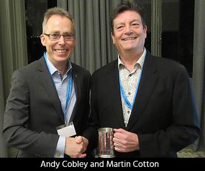 Introducing Martin Cotton as the keynote speaker, Wilkie called upon ICT Chairman Professor Andy Cobley to present him with an inscribed tankard as a token of appreciation for all the support he had given the Institute over many years on the occasion of his retirement from the position of director of OEM projects at Ventec: “The last great adventure for me in the PCB world.”
In his keynote presentation, Cotton challenged his audience to consider laminate dielectric properties in a context of power and cost in a presentation entitled “The Effect of the Dk of a PCB Laminate on the Cost-effectiveness of Office Rental Space. Intrigued?”
Reflecting on a career spanning over half a century, Cotton recalled a conversation with Steve Lloyd, managing director of GSPK Circuits, that had resulted in him offering to demonstrate that the dielectric constant of a material could affect rental costs and power bills as a farewell address to his friends and colleagues in the ICT.
The details of this presentation are reported separately, but suffice it to say that Cotton spoke as an engineer fully trained in value analysis, value engineering, and kaizen, and admitted that although he had rounded, abbreviated, and made shortcuts to show a good story, the outcome held true. No-one disagreed with him.
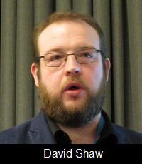 David Shaw, account manager of semiconductor technologies with A-Gas Electronic Materials, gave an update on the Maturolife project, a European Horizon 2020 funded project aimed at coupling design with advanced materials innovations to produce high added value and aesthetically pleasing and functional products for assistive technology, making urban living for older people easier and more independent. The Maturolife acronym translated as “Metallisation of Textiles to Make Urban Living for Older People More Independent and Fashionable.”
The project consortium had 20 partners in nine countries, and the work was divided into two main streams: design and materials science. The design objectives were to embed wants, desires, and aesthetic and emotional responses, ensuring that the end users of the product were engaged in the design process. The material science objectives, as discussed in detail by Shaw, were to develop techniques for the metallisation of textiles based on electroless plating and printed circuit manufacturing processes. At a later stage of the programme, work would be focused on integration of sensors and electronics, production of prototypes, and industrial scalability.
Shaw described a programme designed to achieve sustainable selective metallisation of textiles based on a functionalised copper nanoparticle catalyst and electroless plating to produce superior smart textiles and final finishes to improve the life expectancy of the conductive textile. To enable process development, it was planned to build a pilot line to run in semi-production mode, and eventually to manufacture and validate three assistive technology demonstrators.
Work on test patterns had demonstrated the feasibility of high-resolution metallisation using printed patterns with palladium and silver catalysts as a reference baseline while development of the copper nanoparticle catalyst continued. Significant progress had been made with the copper catalyst, and it was now close to matching the capability of its palladium and silver equivalents.
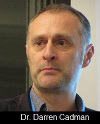 Programme Manager Dr. Darren Cadman from Loughborough University gave an update on the SYMETA project “Synthesizing 3D Metamaterials for RF, Microwave, and THz Applications,” now into its third year. The SYMETA consortium comprised five universities, led by Loughborough and funded by the Engineering and Physical Sciences Research Council. Dr. Cadman explained that the project focus was to create novel, multi-functional 3D metamaterials using emerging additive manufacturing techniques. Metamaterials were materials engineered to have properties not found in naturally occurring materials and were made from assemblies of multiple elements fashioned from composite materials such as metals or plastics. The project aimed to compile a palette of meta-atoms, the basic building blocks of metamaterials, and then to organise these systematically to ensure that the metamaterials demonstrated the required properties.
He reviewed various available additive manufacturing processes—extrusion, jetting, laser sintering, and stereolithography—but commented that these all used single materials, and the project required the use of mixed materials to realise its objectives. He made specific mention of proprietary 3D printing equipment from Nano Dimension and nScrypt, which could work with multiple materials, although the types of UV-curable dielectrics employed tended to exhibit high dielectric loss.
Examples of available dielectric materials for fused filament fabrication (FFF) included FFF PLA (polylactic acid), FFF ABS (acrylonitrile butadiene styrene), FFF PreMix, FFF barium titanate loaded ABS, and PolyJet polymer. And there was a selection of inks available for building conductors including silver pastes, reactive silver inks, reactive organometallics, proprietary silver inks from SunTronic, and Electrifi conductive filament. Copper inks were also available.
The selection of materials for additive manufacturing of microwave devices had to take including their processability in terms of viscosity and flow, curing temperature and adhesion, their reliability in terms of temperature and chemical compatibility, and very importantly, their respective dielectric loss characteristics or electrical conductivity.
Dr. Cadman discussed the synthesis of artificial dielectrics as a means of achieving additional degrees of freedom of material choice and gave examples of various 3D cellular geometries with tailored electromagnetic properties that could be rapidly and straightforwardly fabricated by additive manufacturing. The introduction of metallic inclusions could increase capacitance, at the expense of reducing permittivity. PREPERM had developed a new range of ultra-low-loss thermoplastic materials specifically for improved antenna efficiencies at millimetre-wave frequencies, and these were available in filament form for FFF techniques.
He showed examples of components for X-Band waveguides, prepared on a Voxel8 dual-material printer and demonstrated how relative permeability could be managed by controlling the relative proportions of air-infill and metal-infill. High-dielectric-permeability low-loss ceramic materials were in development at the University of Sheffield, with sintering temperatures below the melting point of silver. Work continued on the optimisation of multimedia extrusion, and it was planned to create microwave demonstrators for operation at frequencies between 10 and 100 GHz.
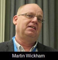 In “Everything’s Getting Hotter! Are High-temperature Electronics Pushing the Boundaries for Solder?” Martin Wickham, senior research scientist at the National Physical Laboratory, discussed the limitations of conventional solders. He also suggested alternative sintered polymeric interconnection materials and described the development of a high-temperature protective coating to enable organic PCBs to operate at higher temperatures. Wickham explained that RoHS2 could create an automatic expiration of exemptions for lead-based high-temperature solders if they were not renewed by requests from industry, and the choice of lead-free alternatives was limited to alloys like tin-antimony and gold-tin for operation above 200°C.
He described an alternative technology developed by the partners in the Elcosint project based on a low-temperature-sintering nano-silver formulation, which would allow a standard SMT production sequence to be maintained but enable operating temperatures of over 250°C. Thermal ageing testing had demonstrated Elcosint to have significantly better reliability than high-melting-point solder at a sustained 250°C, although some of the failures on the soldered samples could be attributed to the high reflow temperature causing degradation of the materials of the PCB.
The outcome of the Elcosint work set a meaningful background to Wickham’s discussion of the results of the Tamessa project. Some interesting observations had been made on conductor cross-sections after long-term 250°C ageing; the copper metal was being progressively converted to oxide. The Tamessa project aimed to create a lead-free manufacturing process based upon standard SMT technology with organic substrates and produce complete electronic systems capable of continuous operation in high-ambient-temperature environments. Substrates and coatings had been developed that specifically inhibited the ingress of oxygen and in high-temperature reliability testing gave results far superior to those achieved with polyimide substrates and coatings and offered a cost-effective alternative to the use of ceramic materials in high-temperature applications.
Work was continuing to understand potential performance enhancements associated with high-temperature coatings and included a review of design rules, improvements in attachment reliability, and the development of a test vehicle to determine the rate of oxidation of inner layers using electrical resistance measurements.
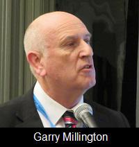 The final presentation was an eye-opener from Garry Millington, CEO of Devtank Ltd, entitled “The Technological Challenges of Designing and Making PCBs for Space.” An RF engineer with 30 years’ experience, the last five of which had been with major contractors in the space sector, Millington identified two main categories within the sector: big space and commercial space. Big space was associated with science missions to outer space, typical satellites in geostationary earth orbit at a height of 22,000 miles, making one rotation per day at a speed of 7500 mph. Commercial space related to satellites in low earth orbit, 200– 1000 miles high, typically making 10–11 rotations per day at speeds around 17,500 mph. The International Space Station fit this category.
A huge commercial project in prospect was the OneWeb constellation of over 800 satellites to provide global broadband internet service to individual customers. And thousands of launches were planned of CubeSats, NanoSats, and PicoSats—very small satellites weighing between 1 and 25 kg—from U.K. spaceports. So, there would be a demand for printed circuits and assemblies suitable for the space environment but at a relatively low cost, creating massive opportunities for the U.K. PCB industry. “In the big space business, you get paid for the paperwork, not the product! This is more commercial stuff.”
But what specific requirements would PCBs and PCB assemblies have to meet for space applications? Millington discussed the mechanical stresses, shocks, and vibrations associated with the launch profile, and the subsequent in-service stresses of vacuum, radiation, and thermal and power cycling.
Two critical items of documentation the PCB fabricator was required to provide were the declared materials list (DML) and the declared process list (DPL). “You need to understand your materials and processes if you want to work with the agencies. You will go through a lot of pain before you get on the qualified suppliers list, but it’s worth the effort once you’re there!”
Outgassing, the release of gases entrapped during manufacture or evaporation of residual volatile material under the vacuum conditions experienced in space, was a major issue—particularly the potential damage it could cause to optical instruments on the payload. Millington showed illustrations of vacuum chamber testing and referenced NASA specifications for materials such as plugging resins. All of these materials were required to be declared on the DML with supporting data sheet information.
Millington listed several other factors that could affect PCB performance in space, particularly the robustness of layer-to-layer interconnections over mission durations. He believed matched CTEs to be essential to avoid failures during temperature cycling. It was important that the dielectric constant of the laminate was stable with temperature and long-term ageing, and breakdown voltages were affected by vacuum. Thermal conductivity was key to heat removal from electronic systems in space because, obviously, there was no air to enable convection cooling. Tin whiskers could not be tolerated, so leaded solders were mandatory together with conformal coating where appropriate.
There were ongoing technology challenges as frequencies continued to rise and structures decreased in size with increases in complexity and power density, requiring more integration and improved heat dissipation. Many of these challenges were similar to those faced in designing 5G infrastructure, and the PCB was no longer just a means for carrying and providing power to components—it was itself becoming a component. Projects were underway to determine the suitability of embedding components in PCBs for space applications and integrating thermal interface materials in the PCB for heat management.
Serial manufacturing of commercial satellites was becoming a reality, using automotive-style production techniques. Millington ended his presentation with a video of a dedicated factory already producing more than two OneWeb satellites daily.
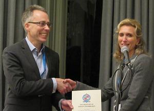
Professor Andy Cobley made closing remarks, thanking the speakers for sharing their experiences, delegates for their attention, and GSPK Circuits for supporting the event, and a special thanks to Bill Wilkie for pulling it all together. Cobley was delighted to take the opportunity to present Victoria Blaisdell, group managing director at Holders Technology, with a certificate to welcome Holders as the Institute’s newest corporate member.
I have been recording ICT events for approaching a quarter of a century, and I never fail to be impressed by the community spirit that exists within our Institute. Although these seminars are offered a technical learning experience primarily, they are much more than that—they are an opportunity for members to get together, network, and communicate on a friendly and informal basis. And, although there may be fewer of us these days, we are still proud to belong to a strong and thriving industry.
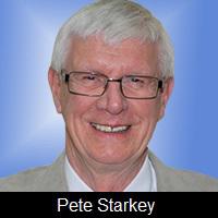
January 2, 2019 | Pete Starkey, I-Connect007