
Institute of Circuit Technology Northern Seminar 2016, Harrogate
A new location for the Institute of Circuit Technology Northern Seminar: Harrogate, the elegant and historic spa town in North Yorkshire, England. And an impressive venue: the chandeliered drawing room of the palatial and stately Majestic Hotel, dating from the Victorian era.
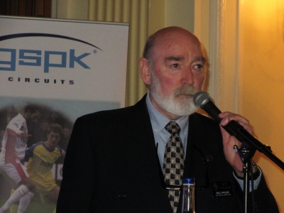 ICT Technical Director Bill Wilkie introduced a programme of four presentations, the first of which came from Martyn Gibson, Operations Director at GSPK Circuits in nearby Boroughbridge, who had sponsored the event. Speaking from forty years’ experience in the industry Gibson, a Lean Champion who had introduced Lean to GSPK and also led a number of customer and supplier initiatives, gave a down-to-earth view of the benefits of lean manufacturing principles in a fast-turn batch manufacturing environment.
Having reiterated the definition of lean manufacturing as an approach for providing products that a customer requires on-time, of the right quality, at the right price, in the right amount, whilst achieving profitability and continually reducing costs, he reviewed the business pressures that justified a lean approach: meeting customer service and quality requirements and extending the company’s reach to global markets, lowering costs, improving operational efficiencies, tracking and controlling material costs, creating a flexible production environment and keeping products aligned to constantly changing market requirements.
He debunked some of the mythology regarding Lean just being about Japanese culture and only applying to the shop floor in automotive manufacture with the objective of cutting costs, and emphasised the focus of Lean thinking - reducing time spent on non-value-adding activities by concentrating on value-adding activities, eliminating waste in all its forms from the whole value stream and continuously striving towards the concept of zero stocks, zero rejects and zero downtime. His rhetorical question was “If your customers could see all the things that go on in your business, would they be prepared to pay for them?” adding “Because they do!”
GSPK recognised five principal elements of Lean: “value” was what customers were willing to pay for, the “value stream” was the series of steps that delivered value, “flow” was the process of organising the value stream to be continuous, “pull” was the act of responding to downstream customer demands, and “perfection” was the result of relentless removal of waste.
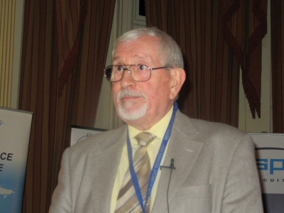 A guru has been defined as "an influential teacher, guide, popular expert, or master of certain knowledge”, and although industry stalwart Dennis Price pretended to be officially retired, it was clear to all present that “enjoying his retirement” necessitated maintaining his links with the ICT network and acting as informal guru to Merlin Circuit Technology.
In his presentation on PCB and chip level heat dissipation methodologies, he began by expressing some concern that a recent designer survey had indicated that heat dissipation was considered a low design priority by many engineers and that the majority of designers did not consider thermal management early enough in the design. More than one in four only considered thermal issues after the design had been completed and more than half only tested thermal design on the first prototype, if at all. And it was the view of many designers that thermal simulation techniques were too complex and time consuming.
Against this background, he explained the basic terminology and principles of thermal modelling, and reviewed the three ways in which heat could be dissipated from a component: by conduction into the PCB, to be spread by the traces or into a heat-sink, by convection into the local environment, either natural or forced and maybe via a heat-sink, or by radiation to any other surface. Conduction and convection were the only realistic methods of heat transfer “except in space where radiation is pretty much all you’ve got!”
Handing round samples from his extensive collection of real examples, Price catalogued the history of development of heat dissipation systems in PCB fabrication technology, from bonded external heat sinks, through copper-invar-copper constructions that served the additional purpose of CTE control, heavy copper single or multiple internal heat planes, to the insulated metal substrates that had become increasingly adopted in recent years. He listed available IMS materials, their suppliers and their data sheet properties, and went on to discuss how they could be utilised in simple single layer designs, and in two layer and four layer constructions incorporating thermal vias and thermally conductive pre-pregs. He also showed examples of double-sided designs with insulated electrical vias through the thickness of the aluminium and areas where the aluminium base had been exposed to enable the attachment of external heatsinks.
To conduct heat away from individual power devices, solid copper “coins” could be bonded into recesses milled into the PCB, and heat could be dissipated from QFN components by mounting them on thermal pads connected to copper planes by thermal via holes, although precautions had to be taken to avoid problems of solder voiding through wicking into them. Price explained how thermal vias could be plugged with thermally conductive resin and plated-over, or completely filled with plated copper. CTE control was still an issue in certain designs and proprietary carbon-core laminates were now being used to replace non-woven aramid composites, which had originally been offered as an alternative to copper-invar-copper but had suffered problems as a consequence of moisture absorption.
Price concluded his presentation with a discussion of developments in the design of heat pipes - capillary two-phase heat transfer devices which effectively worked as closed-loop evaporator-condenser structures transporting heat from a heat source to a heat sink via a volatile liquid, with the waste heat providing the driving force.
 Dr Darren Cadman from Loughborough University is project engineer with the SYMETA project (SYnthesizing 3D METAmaterials), funded by the Engineering and Physical Sciences Research Council. He explained that Loughborough were leading a consortium of five universities and twelve industrial partners, with expertise in engineering, physics and materials science, to develop a range of multifunctional 3D metamaterials with tailored electromagnetic properties for applications in RF, microwave and terahertz electronics.
The project set out to compile a palette of meta-atoms as building blocks for metamaterials, which are synthetic composites with structures that exhibit properties not usually found in natural materials, and to use additive manufacturing techniques to achieve bulk dielectric, metallic and magnetic properties that would open up new innovative opportunities for designers. The aim was to create complex multi-component systems, incorporating elements such as inductors, capacitors, resistors, transmission lines and filters. The ultimate objective was to establish the capability to fabricate all-inclusive PCBs by additive manufacturing, although design for microwave applications, together with materials and processes, clearly presented many challenges.
The established materials for additive manufacturing by fused deposition modelling techniques were acrylonitrile-butadiene-styrene and polylactic acid. New proprietary low-loss polyphenylene ether composites were now available that had been specially designed for RF applications. Dr Cadman illustrated the types of complex three-dimensional cellular structure that could be created, and gave examples of how dielectric and magnetic properties could be modified by the inclusion of metallic elements in the form of disconnected and connected meta-atoms to offer additional degrees of freedom for material choice. A Voxel8 3D printer specifically designed to create electronic devices was being used for initial development work, with multi-material processing as a future objective.
 Professor Karl Ryder from the University of Leicester gave the final presentation, on next-generation surface finishes for PCBs. It was 150 years since Michael Faraday’s statement of the laws of electrolysis and his first experiments in metal finishing. But all of his work related to aqueous solutions. Since the late 1990s, a research group at the University of Leicester had been exploring an alternative approach to metal finishing using non-aqueous chemistry based on a series of ionic liquids consisting of eutectic mixtures of quaternary ammonium salts with either metal salts or hydrogen bond donors. These ionic liquids were effectively room-temperature molten salts which had unusual solvent properties, low vapour pressure and good thermal stability, and many had wide electrochemical windows which enabled results that could not be achieved with aqueous systems. However, they were very expensive, and the team at Leicester had sought to develop liquids that had similar properties but were practicable and cost effective. Mixing ethylene glycol and choline chloride, both readily available in industrial quantities, in 2:1 molar ratio produced a type of ionic liquid classified as a deep eutectic solvent, which had been named Ethaline 200, and this had been used as the basis of a series of metal finishing formulations. Because of its ability to dissolve metal oxides, it had also been demonstrated to have great potential as a soldering flux.
Professor Ryder described applications in electroplating, electropolishing, metal recycling and energy storage before focusing on immersion coatings, in particular metals such as silver, palladium and gold used as solderable finishes on PCBs. Immersion deposition chemistries based on deep eutectic solvents were more environmentally friendly, less toxic and more energy efficient than traditional aqueous processes. The Ionmet project had demonstrated benefits with immersion silver and the Aspis project had shown that the corrosive effects of aqueous immersion gold on electroless nickel could be avoided using deep eutectic solvent chemistry. Moreover, the use of cyanide salts as the gold source was not necessary.
The current multi-partner project, with the acronym Macfest, was nearing completion and the outcome was a nickel-palladium-gold universal soldering and wire bonding finish for PCBs. The base layer was a commercial electroless nickel-phosphorus 3 to 6 microns thick, onto which was deposited a layer of palladium 50 to 150 nanometres thick by a novel immersion process based on palladium chloride in Ethaline. The final layer was 25 nanometres of immersion gold, deposited from an acid-free and cyanide-free formulation where the source of gold could be either gold chloride or sodium gold thiosulphate, again using Ethaline 200 as the solvent. This finish, named ENIPIG had been independently tested for solderability and had shown results as good as or better than standard ENIG, without any evidence of the grain boundary attack which had been shown to cause “black pad” failures with the latter.
Bill Wilkie wrapped up the proceedings, acknowledged the generous support of GSPK Circuits and thanked presenters for sharing their experience and delegates, some of whom had travelled from afar, for their attention and their participation in the question and answer sessions. The formal business over, the informal networking session characteristic of ICT events carried on well into the evening.
Pete Starkey
I-Connect007
December 2016