Institute of Circuit Technology Hayling Island Seminar 2017
Although it is reached by crossing the water over a long road bridge, it is not obvious that Hayling Island, on the south coast of England, is really an island because it is effectively surrounded by natural harbours: Langstone to the west and Chichester to the east. Nevertheless, Hayling Island has become established as the annual venue for an exceptionally popular Institute of Circuit Technology seminar.
 This year’s event had a well-chosen and varied programme featuring presentations on process chemistry and R&D consortia, a discussion of controversial standards proposals and a review of the experiences of commissioning new technology in a start-up factory. As ever, ICT Technical Director Bill Wilkie did a superb job of organising the seminar, welcoming all present, introducing the presenters and moderating the proceedings.
view Andrew Barlow's Presentation.pdf
 Electroless nickel immersion gold finishes have been used on PCBs for over a quarter of a century. The deposition mechanism has been progressively de-mystified, and development continues. Since MacDermid joined forces with Enthone in late 2015 to form MacDermid Enthone Electronic Solutions, the collective expertise of the partnership has been engaged in further research. In the knowledge that Revision A to the IPC4552 specification set an upper specification limit for gold thickness and allowed a lower average gold thickness if good deposit distributions could be achieved, they set out to establish a capable process which would offer potential savings in gold metal consumption. Andrew Barlow described the outcome of this collaborative project, a new proprietary chemistry branded Affinity ENIG 2.0.
He explained that, as gold was deposited by galvanic displacement in the classical ENIG process, the electroless nickel was subject to corrosion from air. And this effect increased with the age of the nickel bath. Key to the new process was a surfactant that inhibited the corrosion and yielded a significantly more uniform gold deposit, even after multiple metal turnovers of the nickel chemistry. The structured development programme had taken a Quality Function Deployment approach to defining and meeting customer needs and was based on six-sigma methodology and statistical process control to minimise process variation. The result was very low panel-to-panel and feature-to-feature variation in gold thickness, which provided a major opportunity for reduction in operating cost.
Barlow demonstrated with standard distribution curves that in accordance with IPC4552 Revision A, which allows a minimum gold thickness of 1.58 microinches at three standard deviations below the average thickness, a tighter gold thickness distribution translated directly to cost saving, and in an actual case study showed that this saving could be almost 30%. MacDermid Enthone were offering to cooperate with customers in joint evaluation and analysis programmes to quantify the benefits of the Affinity 2.0 process.
view Steve Payne's Presentation.pdf
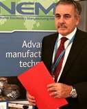 Steve Payne, ICT Vice-Chairman and Manager of European Operations for iNEMI, the International Electronics Manufacturing Initiative, discussed the 2017 iNEMI Roadmap. He explained that iNEMI was a non-profit industry-led consortium of over 90 global manufacturers, suppliers, industry associations, government agencies and universities. It offered its members roadmaps and collaborative projects, together with forums and workshops.
The iNEMI Roadmap was unique in the electronics industry, giving an outlook for the following ten years, updated every other year, with global participation and covering the full supply chain for electronics manufacturing with input from over 500 contributors representing more than 350 companies and organisations. It had become recognised as an important tool for defining the “state of the art” in the electronics industry as well as identifying emerging and disruptive technologies, and helped OEMs, EMS providers and suppliers to prioritise investments in R&D and technology deployment, as well as influencing the focus of university-based research and providing guidance for government investment in emerging technologies
There were two categories of working group: Product Emulator Groups, which covered the "key attribute" needs of the aerospace and defence, automotive, high-end systems, internet-of-things, medical, consumer and office, and portable and wireless product sectors, and Technology Working Groups which forecast evolutionary and revolutionary changes for technology and business infrastructure areas, and identified potential gaps between product sector needs and technology capabilities.
In his first example, Payne discussed the 2017 Roadmap for the internet-of-things product sector, for which two principal market segments of interest were wearables and industrial. The wearables market, with devices worn directly on the body, was perhaps the most visible and with the total world population expected to grow to 7.6Bn by 2019, offered a very large market opportunity. Wearables included smart-bands - focused on activity tracking, identification and gesture control functions, smart watches - particularly as accessories for smart phones, smart glasses and devices enabling virtual or augmented reality, as well as industrial occupational applications. Entertainment and gaming were strong market drivers. The industrial internet-of-things segment offered huge opportunities for connected devices in energy management, industrial controls, safety, quality control, supply logistics and manufacturing control. The roadmap included technology examples and 10-year market forecasts
Critical gaps identified included establishing confidence and assurance on aspects of security, reliability, safety and privacy, ensuring inter-operability between IoT components, particularly across domains, and synchronization across components. And it was clear that the supporting standards lagged far behind applications. There were technology challenges in flexible electronics, batteries and low power high performance processing. Regarding PCBs, the roadmap featured a spreadsheet of key attributes and cost expectations, projected over 10 years.
Payne showed similar roadmap illustrations for medical, and aerospace and defence sectors, before going on to discuss collaborative projects, an example of which was an active initiative aimed at minimising PCB warpage in the assembly process to improve SMT yield.
In his summary, he described the iNEMI Roadmap as an essential tool for strategic decisions for businesses in the electronics sector, looking forward at the technology requirements for all market sectors and relevant to PCB fabricators, suppliers and users. It identified gaps where research was needed and facilitated collaborative projects to address some of those gaps.
It was the publication of Doug Sober’s article in PCB007 on July 10th this year that threw the cat among the pigeons: “Mr. Laminate Tells All: PTFE is about to be banned by IEC TC111” (http://pcb.iconnect007.com/index.php/column/105891/mr-laminate-tells-all/105894)
Doug reported that Technical Committee 111 of the International Electrotechnical Commission proposed a new standard, IEC 63031, defining low halogen materials used in electronic and electrical products, which, if approved, would essentially outlaw PTFE-based materials from use in electronics. The standard was at the Committee Draft Phase, which meant it was being circulated for comment to all the IEC TC111 member countries, and the deadline for comment submission was September 15, 2017.
It was the fact that, other than standards committee members, the PCB industry in general was unaware of the details of the proposal, and was enormously grateful to Doug for making a public issue of it.
view Jim Francey's Presentation.pdf
 Bill Wilkie invited Jim Francey, Sales Manager Northern Europe for Optiprint, to chair an open discussion on the possible consequences, should the proposal be accepted. There was a lively debate around the fact that PTFE was such a ubiquitous material in electronics and electrical engineering, with a unique functionality for which there was generally no practical alternative, that its prohibition would have a huge impact on the electronics industry, and might also set a standard for others such as health care, aerospace, chemical processing and, ironically, environmental protection.
The national committee representing IEC in the UK, hosted by the British Standards Institution, had made its submission before the deadline with the following comments:
“Unless there is scientific evidence that a total mass of halogens greater than a particular value (e.g. 0.9%) is environmentally hazardous then there should not be such a limit contained in the document.”
“Typically, environmental restrictions are based on the properties of a compound / substance rather than the elements forming that compound. Consequently we do not see, unless there is evidence to the contrary, why a limit on elemental halogens is valid.”
“IEC 62474 (Material Declaration for Products of and for the Electrotechnical Industry) contains declarable halogenated compounds that are identified to cause concerns to human health and the environment. It makes sense to use the IEC 62474 database as the single source of halogens that are under this low halogen definition.”
It remains to be seen what might be the outcome.
view Steve Driver's Presentation.pdf
 Introduced by Bill Wilkie as “the prince of the presentations, the lord of the lecture, the doyen of the done deal”, Steve Driver, CEO of the Spirit Circuits group, gave the eagerly awaited final paper – a review of his adventures in Romania and in particular his experiences with the Mutracx “Lunaris” ink-jet etch-resist printing system. He began by referencing and acknowledging the ICT Annual Symposium 2013, when Stuart Hayton’s presentation “The Innovator’s Dilemma – a real-world example in PCB imaging”, had first stimulated his interest in this potentially disruptive technology. Apparently Driver as a schoolboy had a reputation for being disruptive – difficult to imagine! Whatever, he defined a disruptive technology as one that could displace an established technology and shake up the industry, or a ground-breaking product that would creates a completely new industry. As an example he quoted the decline of Kodak from a dominant position in traditional photographic film to filing for bankruptcy protection as a result of underestimating the disruptive potential of the digital camera. And he commented that selling a disruptive concept was not easy – customers did not always know what they needed and preferred the safe bet of hanging on to existing revenue streams and not risking new avenues of opportunity.
But never afraid of taking a calculated risk, Driver’s avenue of opportunity arose when he committed to establishing a start-up PCB factory in Romania, and he summarised his reasoning in choosing Lunaris. In particular, he was effectively starting with a blank canvas – a new factory and new staff, with no pre-conceived ideas of how to make a PCB. The capability of the machine matched his needs and suited his business model of agile manufacturing with reduced lead times. And it offered substantial environmental benefits, which were to his advantage in negotiating permissions and consents to manufacture with the Romanian authorities. Additionally, the machine had the advantages of a small footprint and low power consumption, and it was manufactured in Europe, with local support.
The machine was now in production in Spirit’s BATM Systems factory, Romania’s only volume PCB facility, currently processing about 350 panels per day and it could deliver in excess of 70 good prints per hour, with plans to increase this to 100.
Driver gave a candid review of his experiences, most of which were very positive. Training and support has been excellent and his operators, with no previous experience in PCB manufacture, found the machine simple and straightforward to use. Printing was a proven process and the reliability of the machine had been good, with excellent engineering support from Mutracx. Data preparation and transfer were particularly straightforward, and his CAM engineers had very quickly become expert. Maintenance and upkeep of the machine was an ongoing learning process, for both BATM Systems and Mutracx.
Two major challenges had been encountered, one concerning panel handling and one concerning surface preparation.
The Lunaris had originally been designed as an inner-layer printer, when panel flatness was not an issue because the thin material was held securely on a vacuum table during the printing operation. But BATM Systems were processing 1.6mm rigid material, and if panels were not perfectly flat, or had burrs from panel-cutting or damaged corners from rough handling, a safety mechanism designed to protect the print-heads stopped the machine. BATM’s material suppliers were now aware of the requirement for flat, burr-free panels.
The condition of the copper surface had been observed to have a significant effect on ink adhesion, and pre-cleaning tended to increase ink adhesion to a point where stripping became a problem. BATM Systems were working with their suppliers of laminate and ink to study these effects, optimise the process and establish practicable operating conditions.
Production was predominantly single-sided and the factory was currently dedicated to producing PCBs for LED applications, generally with white solder mask and an OSP solderable finish. All the chemistry from the etching and cleaning lines was treated, regenerated and recirculated in a closed loop system.
Driver was delighted to report that the factory had achieved ISO 9001:2015 accreditation with no non-conformances, and took the opportunity to thank his equipment, material and process suppliers. “The support and interest is humbling, encouraging and appreciated. For Mutracx to continue to be successful the whole supply chain needs to understand the needs of the industry change. Disruptive technologies will disrupt the status quo and bring new challenges to the supply chain and the organisation. Default standards such as IPC are out dated and new supply specifications are needed. Open minds and collaboration with suppliers and customer will make change possible.”
Bill Wilkie wrapped up the seminar, thanking the presenters for their contributions and delegates for their attention. Especial thanks went to MacDermid Enthone Electronic Solutions for their generous sponsorship of the event, which brought together a substantial cross-section of the UK PCB industry for another significant learning and networking opportunity.
Pete Starkey
I-Connect007
September 2017
