|
The Journal of The Institute of Circuit Technology Vol 15 No 3 October 2022 |
|
|
Editorial “Challenges and Changes” |
|
Not so long ago in a galaxy far away, the ICT Incorporated under the 2006 Companies Act. We did this in 2009 and as an example of how fast the Industry is moving, it was only two years earlier that a young guy called Jobs demonstrated a new phone at an electronics fair in the US. In 2007, a Finnish company called Nokia ruled the roost as far as mobiles were concerned, making more mobile phones than anyone else in the world. Their expertise came from antennae design, shaped no doubt by the need for good signals in the mainly mountainous terrain. A young designer had been able to get a meeting with the Nokia board and showed them how pages could be scrolled, which was an innovation at that time. Nokia had been getting away annually with small changes in design and a large uplift in prices and this had fueled complacency and bloated employee benefits for the thousands who worked locally. They explained that customers didn’t want changes and that they were big and he was small. That same year, one of the Nokia directors was recalled to base, to be told that they had just witnessed Steve Jobs of a start-up company called Apple, demonstrate a new iphone and it looked light years ahead of the new Nokia. Not only that, it featured full-page scrolling. Within two years Nokia were second to Apple and now Nokia have returned to making Antennae and Apple is worth 2 trillion dollars. At about the same time, Blockbuster Video dominated the home video market and had an opportunity to buy Netflix for 50 million dollars. Their new CEO, John Antioco perceived that their business model of having families visit bricks and mortar stores in person was better than a postal system using DVD’s and turned them down. Now Blockbuster Video is no more and Netflix is one of the largest companies in the world. You could argue that John made a decision based on the facts he had available, but he is forever known as the guy who turned down Netflix. If all these changes have happened in the last 15 years, think what the next 15 will bring! |
| Section 2 | Calendar of Events | |
Bill Wilkie |
2022 |
Details |
| Nov 29th | Evening Seminar at Meriden Preceded by Council Meeting and Fabricator Meeting. Evening Seminar starts at 18:00 – to be followed by a buffet. Manor Hotel Room Rate - £100/night B&B at ICT Rates | |
|
September 7, 14, 21, 28 and October 5, 12, 19, 26 |
On-line Engineering Training with Happy Holden. Each session is from 4pm to 5pm | |
| June 8th | Annual Symposium | |
| April 11th - 14th | Annual Foundation Course | |
| March 22nd |
AGM and Webinar Meeting |
|
| Go back to Contents | ||

|
Synthetic Graphite: A New Solution for PC Board Thermal Management |
|
 John Priday, John Priday, Chief Technical Officer, Teledyne Labtech |
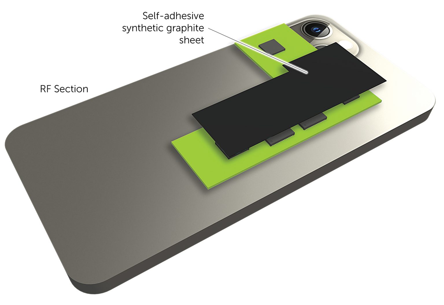
1. Introduction Figure 1: Typical smartphone RF section showing the use of a synthetic graphite pad to aid thermal management Some of the most acute heat management challenges are seen in aerospace and defence applications. Usually these have an extreme focus on system size, weight, and power (SWaP), which makes heat management an even more critical topic. Such applications will typically sacrifice low cost to achieve the highest performance combination of thermal management, signal fidelity and size/weight. Examples include power amplifiers, phased array transmit/receive (Tx/Rx) modules and high speed digital processing cards. The most effective heat dissipation technique we’ve found for power devices is the use of copper coins. However, we wondered whether the benefits of synthetic graphite could be leveraged for SWaP-constrained medium power applications. Our concept was that PCBs use sheets of copper as ground planes. Could these be replaced with synthetic graphite instead? 2. Why Care About Synthetic Graphite? 3. Requirements for Using Graphite Planes in PCBs
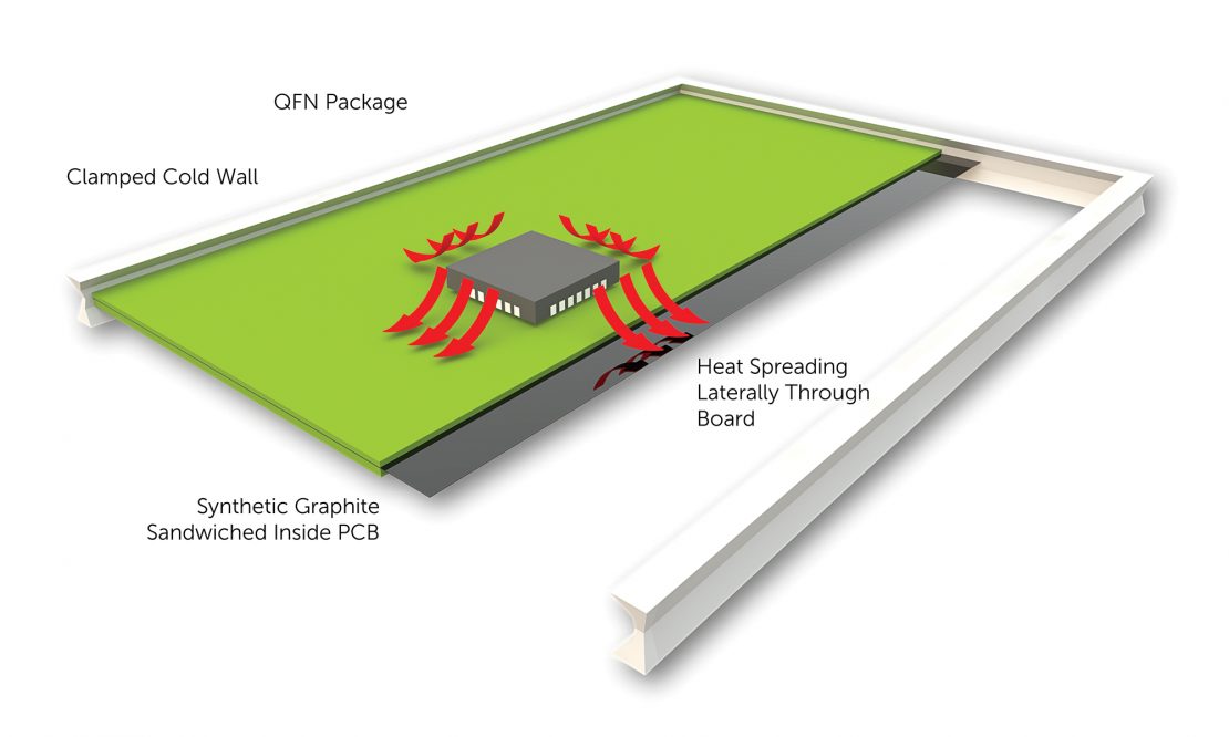
Figure 2: Aerospace card application with a QFN packaged high power device on a PCB. Thermal management is aided using cold walls and board clamps to allow heat to be moved into the enclosure. The use of thermal graphite would be beneficial if a suitable approach could be found to accomplish it. This is typically achieved through mounting devices on thermal/ground pads on the top layer of the PCB. These are then electrically and thermally connected to lower layers through plated through-hole (PTH) vias. Sometimes these are filled with solder, but more often with thermally conductive filler. To replace copper planes in the PCB sandwich, graphite would have to perform well in several areas to be worth pursuing: 1. Have enough thermal advantage to be worth the effort. 4. Development of Graphite-Layer PCBs
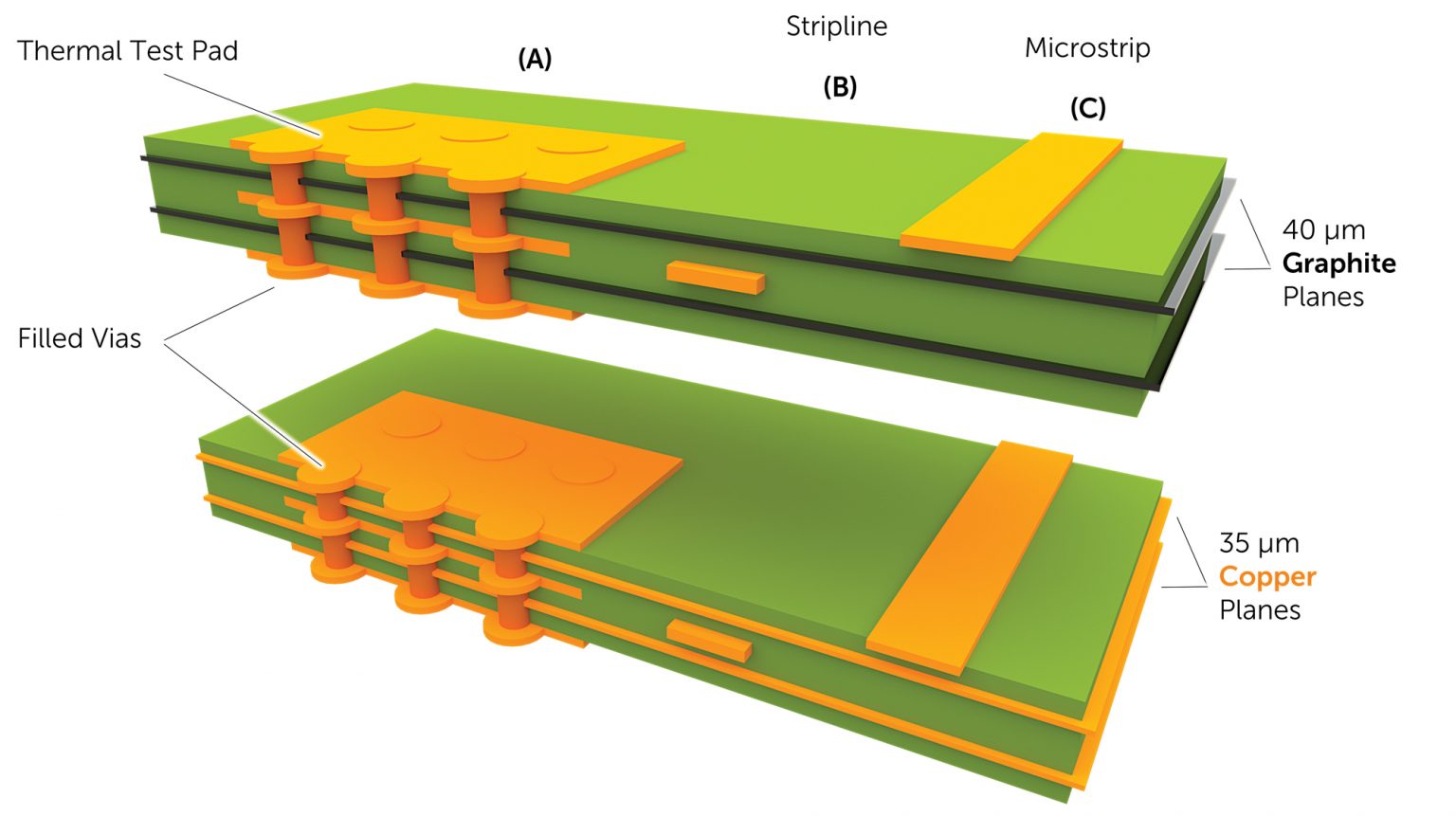
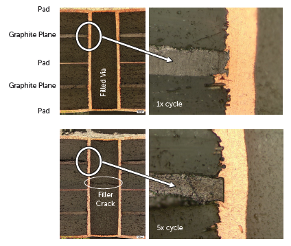
Figure 3. The two test boards, one using synthetic graphite planes, the other substituting copper planes 5. Evaluation Tests were performed with 1 cycle of 10 seconds solder float at 288°C and then five cycles starting from ambient room temperature for each cycle, all of which were successfully passed. The only notable degradation seen was in the via filler that cracked after five thermal stresses, which was the likely result of coefficient of thermal expansion (CTE) mismatch but was not considered significant. See figure 4 below.
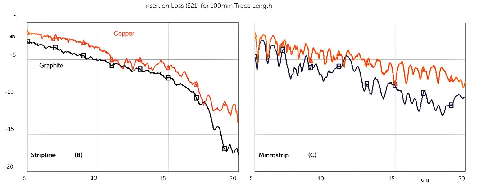
Figure 4: Pass Result after Five Thermal Cycles to 288 oC Having shown that graphite can be incorporated into a PCB and survive thermal shocks, the most important question is then whether it actually improves heat dissipation. To explore this, a power resistor was mounted on both PCBs using H20E conductive epoxy to act as a heat source. Thermal measurements were made using a Teledyne FLIR infrared camera. In both cases, the same power (6.7 W) was applied and allowed to stabilize for 5 min. The boards were suspended in the air with no additional heatsinking. The resistor was more than 20° C cooler in the graphite-plane case compared to the equivalent using copper planes. This would significantly improve the Mean Time Between Failure (MTBF) reliability of a semiconductor device in normal use. For this new heat mitigation material to be useful, it could not substantially degrade signal integrity, so to evaluate microwave performance, the test structures had both stripline and microstrip test paths. To make measurements, 10mm aluminium plates were bonded to the back of the PCBs to allow for mounting of SMA connector interfaces. A vector network analyser was used to conduct measurements from 5 to 20 GHz, and the results are shown in Figure 4 for both stripline and microstrip test structures. The graphite planes caused a maximum degradation in insertion loss of no more than 2 dB. This was for a 100mm trace length, which is two to three times that of the typical total length of the signal path on most PC boards. For many applications, this performance will be more than acceptable. It should be noted that for results above 18 GHz, the stripline was not optimal because of the mismatch of the connector interface.
Figure 5: Measurements from 5 to 20 GHz of insertion loss (S21) for stripline (left) and microstrip (right) 6. Summary 1. Graphite-plane PCBs do have enough thermal advantage to be worth the effort, keeping a component more than 20 °C cooler in our example experiment. Synthetic graphite offers a significant weight saving and offers benefits in terms of thermal management for PCBs that have medium power devices mounted on them. It’s ability to carry and distribute heat efficiently in the X-Y plane, that can be taken out to the perimeter of the PCB and then extracted via clamps to a cold wall will be attractive for some applications. The additional benefit of allowing semiconductor devices to operate at substantially reduced stabilised temperatures will also enable improved MTBF predictions for PCBAs. There are certain restrictions as a result of the necessity to maintain via integrity and we would strongly recommend early stage discussions with your supplier to ensure all design for manufacture considerations are included.
|
| Section 4 |
Selective Soldering: A need for Innovation and Development Samuel J. McMaster*1, Andrew Cobley, John E. Graves, Nigel Monk2 |
||||||||||||||||||||||
 Dr Sam McMaster Dr Sam McMasterMaterials Scientist (KTP Associate) Pillarhouse International |
1. Introduction
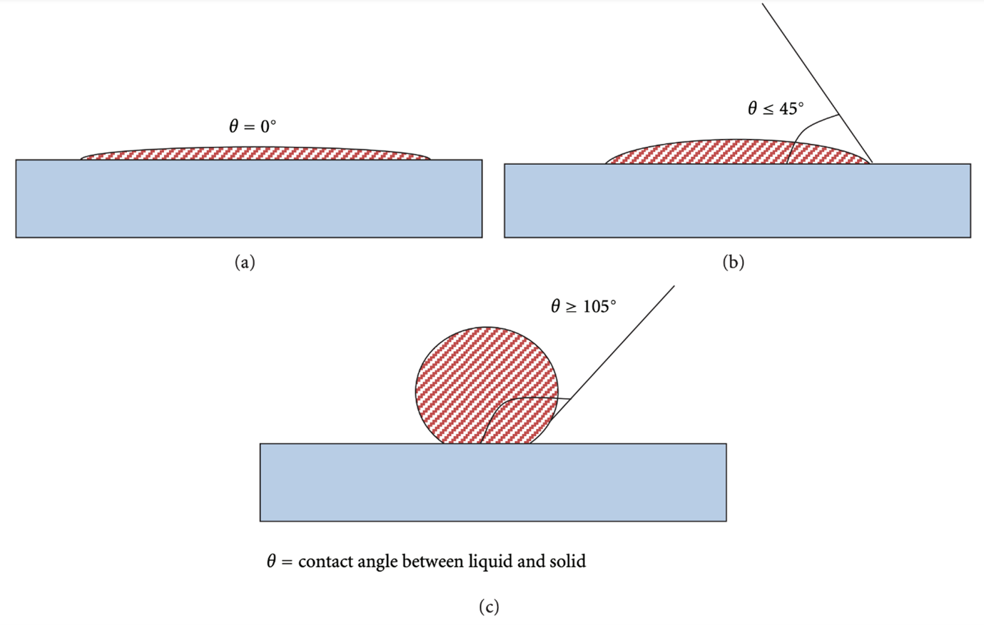
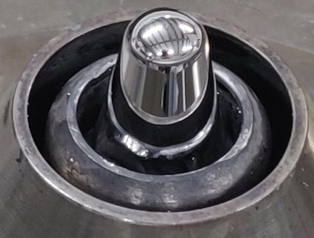
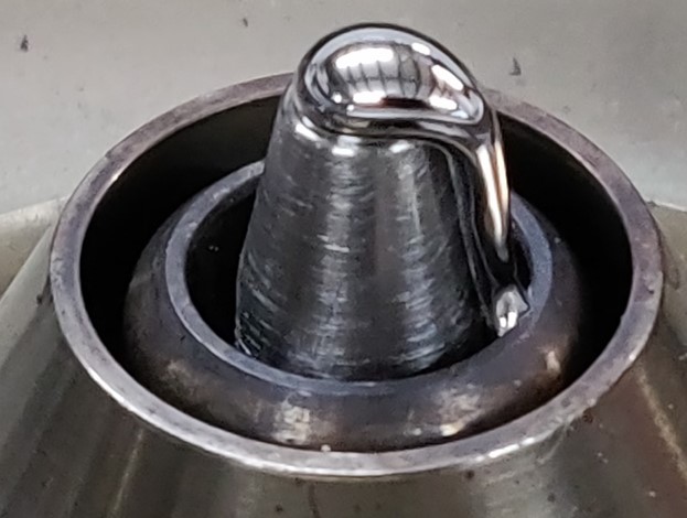
Figure 3. An example of a wetted nozzle.
For wetting between the liquid solder and the nozzle, there must be a clean interface with minimal surface oxides on the nozzle. The presence of oxides on the surface interferes with the wetting of the solder to the surface by acting as a barrier; additionally, the surface energy of oxides is too low for wetting to occur. Flux is used to remove oxides and generate/maintain this clean interface before and during operation. After cleaning, a chemical reaction between the solder and nozzle determines the extent of the wetting but this interaction also limits the lifetime of the nozzle. It causes wear of the nozzle and metal is leached into the solder bath. Exposure to the solder and the subsequent reaction alone does not cause significant wear. The contribution of liquid flow increases the wear in a synergistic effect which suggests that the underlying mechanism is complex corrosion-erosion.
Indexes |
||||||||||||||||||||||
| Section 5 |
Solder Joint Reliability in Light Emitting Diode Modules Professor Martin Goosey |
|||||||||||||||||||||
|
Prof Martin Goosey |
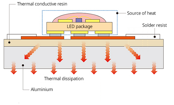
The key to achieving good reliability and requisite service lifetimes in modern electronic devices has long been associated with the quality of the solder joints used in assembling components onto substrates. The electronics industry originally used leaded components with through hole mounting and solder joints that were much larger than those currently used. The solders were alloys of tin and lead with modest melting points and good mechanical properties. However, progress in electronics has always been characterised by greater levels of integration and miniaturisation and these required a move to surface mount technology with increasing numbers of connections per unit area on a substrate. As a result, the volume of solder used in solder joints has significantly diminished, e.g., in area array packaging. The use of tin-lead solders has also been proscribed. The commonly used replacement lead-free solders, typically have higher melting points, form different intermetallic compounds and have mechanical properties that can impact solder joint reliability when compared to conventional tin-lead solders. While this evolution in technology has been extensively studied, it is acknowledged that, for some applications, solder joint reliability can still be a very significant factor. This is particularly the case where devices are exposed to extensive thermal cycling, or extreme variations in operating temperatures. Such conditions were typically associated with military and aerospace electronics applications. However, the more widespread adoption of Light Emitting Diode (LED) technology in all types of consumer, professional, automotive and industrial lighting is another area where solder joint reliability is now a very important issue. Although individual LED lighting designs vary significantly, they are all typically based on the use of compound semiconductor devices assembled onto a suitable substrate using solder. Solder joints are a vitally important part of these assemblies, as they have to provide a stable and reliable current path, as well as contributing to the requisite cooling of the chip via good thermal contact to the underlying substrate and heat sink.
As LEDs often generate a large amount of heat as well as light, these assemblies become hot in use and thus experience significant thermal excursions between their ‘on’ and ‘off’ phases. This thermal cycling can have a major impact on solder joint reliability and lead to early failures. Operating at high temperatures also negatively impacts their light outputs, as well as shortening the service lifetimes of such devices. It has been reported for example that, in some cases, up to 80% of the energy input is converted into heat, while every 10 °C increase in temperature can decrease the lifespan of an LED by as much as 50 %. With the growing demand for brighter, higher density LED lighting arrays, the need for improved thermal management has become increasingly important in order to enable operation at more acceptable temperatures and to provide the requisite service lives.
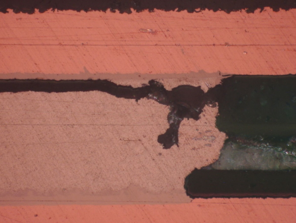
Cracking of Solder Joint From Thermal Stress Manufacturers of electronics have long understood that solder joint reliability is, at least in part, significantly impacted by the materials used in electronic assemblies and, in particular, by their thermal expansion characteristics. Materials such as silicon, copper and glass-filled epoxy resins all have markedly different coefficients of thermal expansion which, when combined in a device that experiences extensive thermal cycling, expand and contract at different rates, creating stresses which ultimately impact the solder joint reliability. In conventional electronics, these materials are typically copper, FR4 epoxy-glass fibre laminates, lead-free solder and perhaps a packaged silicon device such as a flip chip or ball grid array etc. assembled onto a substrate. However, in the case of the LED assemblies used in lighting modules that exhibit a high heat output and experience substantial thermal cycling, substrate manufacturers have produced a variety of Insulated Metal Substrates (IMS) that utilise combinations of metal cores along with the use of thermally conductive ceramic fillers in the dielectrics. Due to its relatively low cost, aluminium is the preferred metal employed in IMS for LED and related applications, but it also, unfortunately, has a significantly higher coefficient of thermal expansion (CTE) than copper, (23.6 ppm/ºC versus 16.6 ppm/ºC. This higher CTE, coupled with the need to use as thin a layer as possible of dielectric between the aluminium and the copper interconnects is one of the key reasons why there is the potential for a negative impact on solder joint reliability during thermal cycling. There are, effectively, a range of materials expanding and contracting over a comparatively large area in the LED assembly and it is now widely recognised that this ultimately impacts solder joint reliability. Solder joint reliability is thus one of the main failure mechanisms occurring in LED modules.
Typical LED Assembly for Heat Dissipation There has consequently been a lot of work carried out to establish what can be done to prevent, or minimise, solder joint failures in such applications. Although the basic reasons for, and mechanisms of, thermal cycling induced solder joint failures are well known, the situation with LEDs is also subtly different and potentially much more complex. True solutions require a good understanding of these mechanisms, so that the knowledge can be used to inform both the specific material choices and the ultimate designs actually employed. Although thermal cycling induced solder joint cracking is related to the use of materials with markedly different thermal expansion coefficients, the situation with LED lighting may be somewhat different from that encountered with more traditional conventional electronics. This is because the use patterns and rates of heating and cooling are often more rapid. As an LED device is turned on, it rapidly warms up to its steady state operating temperature, causing the various materials it contains to expand to different degrees. The solder connecting the LED to the substrate is bridging less-flexible materials with different expansion coefficients, i.e., typically the substrate and the LED device and this results in an induced strain in the solder itself. What exactly happens within the solder joint depends on several factors, including the elemental composition of the solder alloy, its structure, the rate of heating and the ultimate temperature increase. If the increase and decrease in temperature is rapid, i.e., via a short on off cycle, the solder joint will exhibit an elastic and potentially reversible deformation. However, over longer periods, the elastic deformation will be followed by a slower plastic deformation, as the solder effectively starts to flow under the load. This is known as solder creep and will continue until the thermally induced strain has been eliminated. On cooling, the joint will not revert to its original shape, as there will have been irreversible changes in the microstructure of the solder alloy. Cooling thus results in the generation of further stresses in the joint, which will also tend to be eliminated by solder creep. The on-off cycling of the device leads to repeated cycles of loading and creep in the solder joint. Ultimately, this results in fatigue cracking being initiated in the solder, with the cracks typically propagating along any discontinuities in the joint, such as where there may be brittle intermetallic compounds of silver and tin or copper and tin (depending on the specific solder etc.) within the bulk of the joint. In the case of SAC (SnAgCu) alloy solders, recrystallization of large tin grains can occur across the high strain regions of the joint which can then be followed by crack growth along the resulting network of highly angular grain boundaries.
Solder Joint Failure In addition to the microstructural changes induced during heating and cooling, there may also be microstructural changes due to the evolution and growth of the intermetallic compounds (IMCs) in the joint. The main IMC layer is formed at the interface between the solder and the copper on the IMS during the soldering assembly operation and it continues to grow during any further thermal excursions. The thickness of the IMC and the nature of the interface are both known to have a significant impact on overall solder joint reliability. Other important factors that can impact the quality of the solder joints formed include the solderable finish applied to the copper. This might, for example, be a nickel-gold coating, in which the gold dissolves into the solder joint during soldering, but may which then precipitate in the joint on cooling. The actual quality of the soldering process used in the assembly of the devices is also critical, as the formation of voids within the solder can lead to premature joint failure. Void formation is influenced by the type of solder paste and fluxes used. As the quality of the interface bond area between the chip and substrate essentially determines the effectiveness of the heat dissipation, porosity and voiding will lead to an increased thermal resistance and thus elevated LED chip temperatures that cause accelerated ageing. It can thus be seen that the unique operational nature of LED lighting modules can make them susceptible to solder joint failures and yet they are required to operate with good long-term reliability, often in harsh conditions. The key question, therefore, is what can be done to help minimise or even eliminate solder joint failures in these devices. Clearly, given the thermal cycling that occurs and the use of a range of disparate materials, there are opportunities for suppliers to develop materials that help to minimise the impact of differential thermal expansion during thermal cycling. One obvious approach is to build some compliance into the substrate materials via the dielectric layer that separates the solder joints from the underlying aluminium layer. For example, by using a specially formulated dielectric with a low modulus, it is possible to reduce the force generated by expansion of the underlying aluminium. Pure aluminium has a coefficient of thermal expansion (CTE) of around 23.6 ppm/ºC, although the alloys used in this type of application, e.g., 5052, have slightly higher values. The key point is that, compared to copper (16.6 ppm/ºC), the CTE is relatively high. Also, in terms of what actually ultimately controls the overall stresses and expansion, the aluminium in the IMS is by far the thickest component, which means that its expansion dominates the dielectric layer and the copper. This can easily be demonstrated by comparing the measured thermal expansion coefficient of aluminium 5052 with that of a typical IMS substrate. The aluminium 5052 will typically have a value approaching 25.0 ppm/ºC. However, for a typical IMS substrate, which might comprise a 1.5 mm layer of aluminium below 100 µm of dielectric and a top 35 µm thick copper layer, the measured expansion coefficient only reduces very slightly to a value of 24.0 ppm/ºC. Clearly, it is the relatively thick layer of the aluminium that dominates the overall measured expansion coefficient of the substrate. Given that the aluminium thickness needs to be maintained in order to provide the levels of thermal conductivity, any opportunity to prevent the large expansion of the aluminium impacting the solder joints is limited to the dielectric material between the aluminium and the copper.
Example IMS material, thickness and thermal conductivity values (* pure metal)
Martin Goosey |
|||||||||||||||||||||
| Go back to Contents |

|
Automation and the Journey to your Smart Factory Happy Holden |
|
|
Happy Holden |
During September and October we have been holding a series of on-line engineering sessions presented by Happy Holden. These are based on his book "Essential Skills for Engineers" This series of presentations were free to members and guests and is a valuable resource for in-house training of engineers and their career development. The sessions have gone extremely well and have attracted delegates from a wide range of our industry. We will summarise the contents in our next Journal. The webinars will be available on the ICT website for future reference for those who did not catch the live sessions
|

|
Members News |
|
|
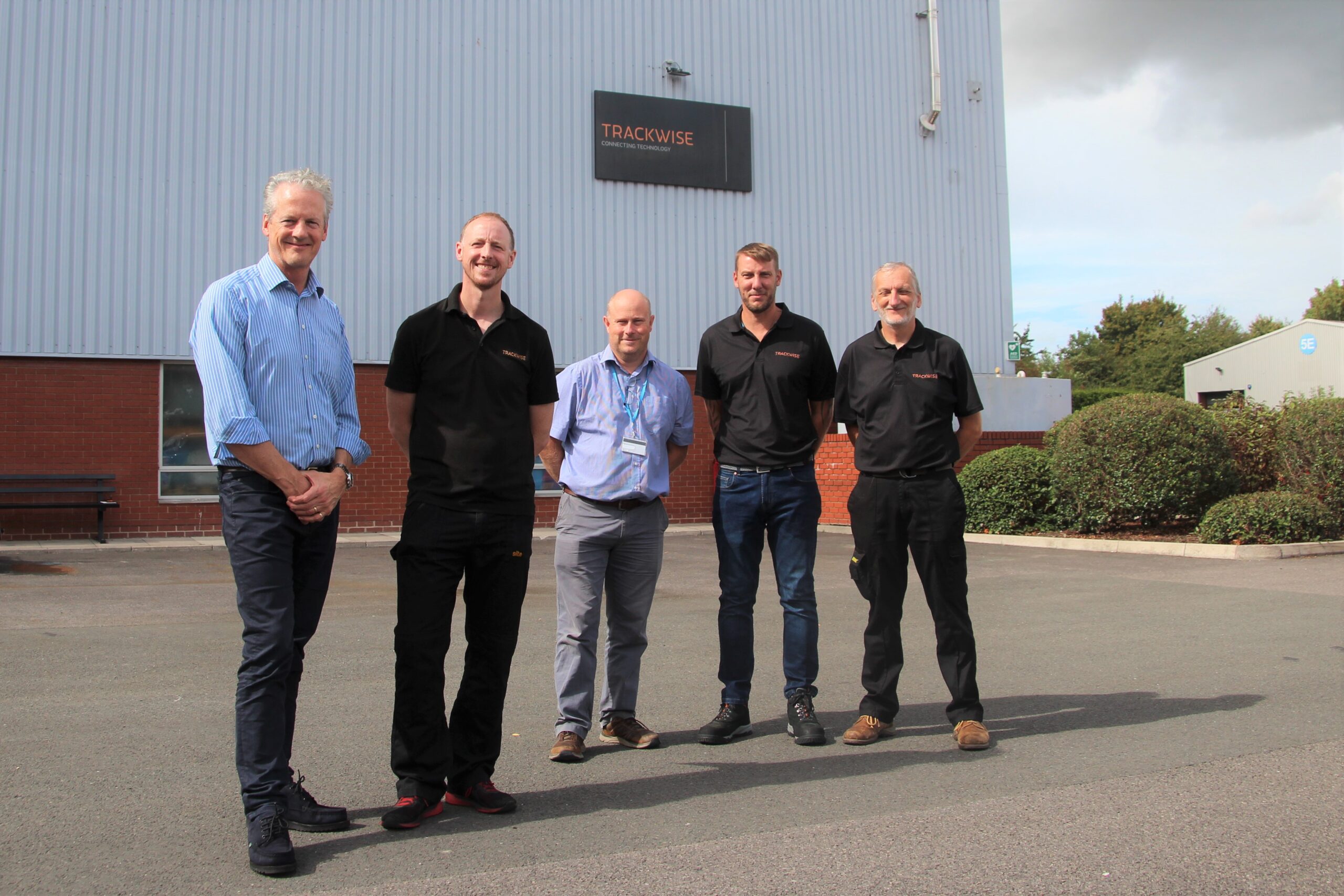
Trackwise employees recognised for nearly a centenary of service. With a combined length of service close to 100 years, there’s very little Ben, Mike, Nigel and Marc don’t know about the manufacture of flexible printed circuits. Read more... |
|
|
|
Mike Devine
My sincere condolences to you, the family and all your beloved ones, Ellie. I was truly sad when I heard the news. Having known Mike for more than 20 years I can only believe that he will leave a huge gap for you all. Mike's knowledge of printed circuit manufacturing made him old school Royalty in our industry. In business he was always the true gentleman in several roles he has had from Thomas Walters to ExceptionPCB. I wish you and all your beloved ones the strength to live with this enormous loss. The PCB industry has lost a Giant. |
|
Alex Gordon 1939-2022 He’ll be sadly missed. |
|
|
|
 For and on behalf of my father, Mike Devine. It is with a heavy heart to announce his passing on Sunday 14th August.
 Alex was a regular delegate at ICT events in the 80’s and 90’s and took particular interest in many of the Environmental Best Practice Projects prevalent at that time.
|
Industry News |
|
| Amphenol Invotec | Amphenol Invotec awarded Nadcap Merit Status across both UK sites. The Amphenol Invotec team are celebrating having been awarded #Nadcap Merit Status across both UK sites. Nadcap merit status signifies superior performance during the stringent auditing process and highlights the outstanding quality processes that have been implemented to the aerospace supply chain. Read more... |
| Eurotech |
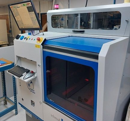
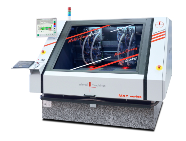
Eurotech Group invest in a new Schmoll Laserflex.
|
| Graphic | Graphic plc awarded Nadcap accreditation with merit Read more... |
| GSPK |
GSPK - The only UK PCB Manufacturer with Automotive Accreditation IATF16949-2016
|
| Newbury Electronics |
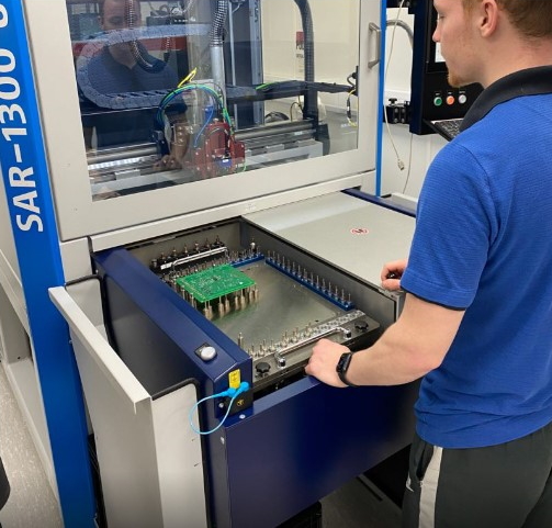
After years of cropping and cutting, the photos show our new Schunk SAR1300 depanelling machine. A previously much disliked manual task is now automated, with magnetically fixed tooling pins placed automatically. Read more... |
| Ventec |
New Flex Rigid Material for Critical Applications
|
| Zot |
Zot Invest in a new Schmoll Router
|
| Go back to Contents |


Membership News |
|||||||||||||||||||||||||||||||||
|
|
New Corporate Member
|
||||||||||||||||||||||||||||||||
|
New Member
|
|||||||||||||||||||||||||||||||||
|
Regrading Associate to Member
|
|||||||||||||||||||||||||||||||||
|
New Honorary Members
|
|||||||||||||||||||||||||||||||||
|
For Outstanding service and support for the Institute – Honorary Member
|
|||||||||||||||||||||||||||||||||
|
Member to Fellow
|
|||||||||||||||||||||||||||||||||
| Go back to Contents | |||||||||||||||||||||||||||||||||
ICT Council Members |
|
|
Council Members |
Emma Hudson (Chair), Andy Cobley (Past Chairman), Steve Payne (Hon Deputy Chairman), Chris Wall (Treasurer), William Wilkie (Technical Director, Hon Sec, Membership & Events), Richard Wood-Roe (Web Site), Lynn Houghton (Hon Editor), Jim Francey, Martin Goosey, Lawson Lightfoot, Peter Starkey, Francesca Stern and Bob Willis, |
Editors NotesThe ICT Journal |
|
|
Lynn Houghton |
Instructions / Hints for Contributors 1. As it is a digital format the length is not an issue. Short is better than none at all! 2. Article can be a paper or a text version of a seminar or company presentation. Please include data tables, graphs, or powerpoint slides. We can shrink them down to about quarter of a page. Obviously not just bullet points to speak from. 3. Photo's are welcome. 4. We would not need source cross references 5. Title of presentation - Of course! Date, Job title of Author and Company represented. 6. An introductory summary of about 150 words would give the reader a flavour of what it's all about. 7. Style - we don't want out and out advertising but we do recognise that the author has a specialism in the product or process that will include some trade promotion. Sometimes it will be a unique process or equipment so trade specific must be allowed. 8. Date and any info relating to where or if this article may have been published before. 9. We can accept virtually any format. Word, Powerpoint, publisher, PDF or Open Office equivalents. 10. Also, to make it easy, the author can provide a word file to go along with his original powerpoint presentation and I/we can merge it together and select the required images. 11. A photo of author or collaborators. I really do look forward to receiving articles for publication. Lynn Houghton |