The Journal of The Institute of Circuit Technology

Welcome to our latest Technical Journal. The journal is published quarterly and distributed to Industry Experts. 

We invite you to join our mailing list and be part of our aim of disseminating and publishing technical and training information for the greater benefit of our industry. This is a complimentary subscription with no commitment.  

Subscribe to The Journal. The next issue will be sent to you in April 2023

   
ict logo

The Journal of
The  Institute of Circuit Technology
Vol 16 No 1
January 2023


Links to Contents 

  Author  Section
Editors Introduction Richard Wood-Roe 
Calendar of Events Bill Wilkie  2
IPC Warning about Microvia Reliability for High Performance Products Happy Holden 3
Process Improvement Strategies for Weak Microvia Interfaces William Bowerman 4
Ultra Thin Base Materials Take PCB Manufacturing to the Next Level Daniel Schulze  5
Computer Aided Engineering Simulation for Production Proofing PCB Copper Plating Robrecht Brelis  6
The ICT Christmas Seminar 2022: The Calibre of a ‘World Cup’ Event Pete Starkey   7
Members News: Bill Miller - Obituary 8
Industry News:  9
Membership Update:  New Members and Grading  10
Corporate Members

11

Council Members 12
Editors Notes Richard Wood-Roe 13


Section 1 Editors Introduction

rick profile2

Richard Wood-Roe
Journal Editor

In this issue of The Journal we have included an update to the IPC alert about microvia reliability from Happy Holden. There is a paper outlining the optimisation of process parameters for microvia processing from Bill Bowerman of Alpha Macdermid. Daniel Schulze of Dyconex has provided a fascinating contribution detailing the benefits of thin materials for space saving and reliability. Computer Aided Engineering Simulation for Production Proofing PCB Copper Plating is the subject of a paper from Robrecht Brelis of Elsyca. We are grateful to Pete Starkey for his write up of the recent ICT evening seminar that was held in Meriden, West Midlands. In the members news section we report on the sad passing of Bill Miller, a founding father of the UK PCB industry. The members update section shows a large increase in members from the successful on-line engineering course. This course will be available again soon via our web site. Finally the industry news section highlights the activity of some of our members.

  Go back to Contents


Section 2 Calendar of Events 

bill wilkie

Bill Wilkie
Technical Director and Membership Secretary

           2023

            Details 

March 7th ICT AGM and Spring Seminar at Meriden. 

Council Meeting – Starts at 12 noon, Fab Group Meeting starts at 14:30, AGM/Seminar starts at 18:00 – to be followed by a buffet.

Manor Hotel Room Rate - £100/night B&B at ICT Rates

April 24-27th Annual Foundation Course, Chester
2022  
Nov 29th Evening Seminar at Meriden Preceded by Council Meeting and Fabricator Meeting. 

September 7, 14, 21, 28 and October 5, 12, 19, 26

On-line Engineering Training with Happy Holden. Each session is from 4pm to 5pm
    Go back to Contents


Section 3

IPC Warning About Microvia Reliability for High Performance Products
Happy Holden
Updated: April 15, 2020

Editors Note: It is recognised that this alert was issued some time ago but it has been included in this issue of The Journal to ensure that members who may have missed it are informed.

 fig 1Happy Holden 

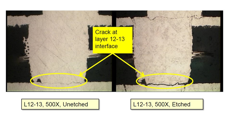
Hopefully, by now, you have read the full Press Release from the IPC on March 6, 2019, about the warning of field and latent failures of high-profile HDI boards. IF not, the complete press release is available on I-Connect 007. [1]

What you may have seen is the warning statement which the IPC will be including in the upcoming IPC-6012E, Qualification and Performance Specification for Rigid Printed Boards:

“There have been many examples of post-fabrication microvia failures over the last several years. Typically, these failures occur during reflow, however, they are often undetectable (latent) at room temperature. The further along the assembly process that the failures manifest themselves the more expensive they become. If they remain undetected until after the product is placed into service, they become a much greater cost risk, and more importantly, may pose a safety risk.”

DON’T PANIC! Let me explain the background of this warning.

For the last few years, a few OEMs have experienced a latent defect in their sophisticated HDI multilayers even though screened with our best available incoming inspection and test methodologies. This defect caused failures observed in:

• Post-Reflow In-Circuit Test
• During the “Box Level” Assembly Environment Stress Screening (ESS)
• When removed from storage
• In-Service (End-Customer Fielded Product)

After much work and investigations by these OEMs, and with coordination with the D-32 Thermal Stress Test Methodology Subcommittee, the IPC issues a new test method for thermal stress, (IPC-TM-650, Method 2.6.27A) and thermal shock (IPC-TM-650, Method 2.6.7.2). The Method 2.6.27 calls for the test vehicle or coupon to be subjected to a normal solder paste reflow profile to reach a peak temperature of 230 degree C or 260 Degree C while under connection to a 4-wire resistance measuring unit for six (6) full reflow profiles without the increase of resistance of 5%. The daisy chain in the test coupon needs to be composed of features used in the actual circuits.

This has allowed these OEMs to detect the latent microvia failures and protect themselves from possible defect escapes. But finding the Root Cause of this latent HDI failure has been elusive. So, in early 2018, the IPC organized a select group of industry experts, under the supervision of Michael Carano, to investigate this situation. Later in 2018, this group was named the IPC V-TSL-MVIA Weak Interface Microvia Failure Technology Solutions Subcommittee. I am a founding member of this group. But let me emphasize,

During the past year, we have met and gone over test data, microsections and experimental results. Here is what we KNOW:

• The defect manifests itself as a fracture at the metallurgical interface of a microvia to the copper layer below it or to another microvia below it. (see Figure 1)

fig 3

FIGURE 1. The WMI latent defect observed after six reflows of 230 OC. [used with permission][4]

• First occurrence of the product-level failure detected (stacked microvias) 2010.
• Complex stacked microvias can exhibit this latent defect (>2 stacks) but not staggered microvias.
• Data thus far implies stacked microvia structures, especially stack-heights of 3 or greater, are much more likely to suffer this failure mode, and it is still a minority (but growing) percentage of high-reliability designs.
• Severity of end-use application environment (which we attempt to address by severity of test condition) appears to have some impact on the likelihood of occurrence.
• Several OEMs allow stacked FILLED vias if the design is no more than 2. Three is the tricky one.
• This has been observed in complex HDI structures such as the 3-8-3 Qualification Coupon Design seen in Figure 2 below.

fig 4

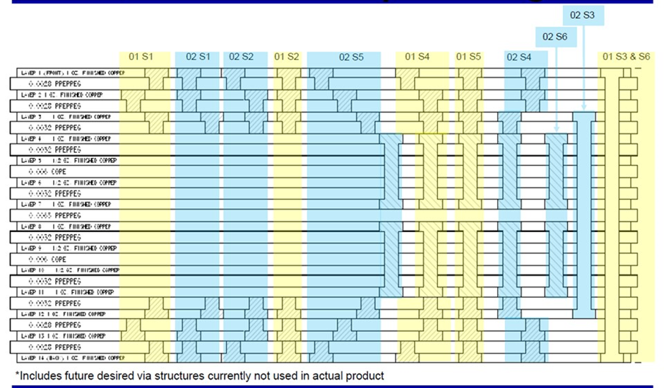
FIGURE 2. A complex HDI qualification coupon (3-8-3) with both stacked and staggered microvia structures. [used with permission] [4]

• Product-level failures are unpredictable (in-process, storage or filed)
• Historical industry-standard test methods were insufficient in detecting this failure but seem sufficient for normal HDI constructions.
• Preconditioning and thermal cycling may induce this defect but when it returns to room temperature, the defect is not detectable by 4-wire resistance measurements. Only when the PCB is brought up to reflow temperatures is it apparent.
• IPC TM-650 2.6.27A technique that duplicates assembly reflow will reliably detect this latent problem. (see Figure 3 below).

fig 5

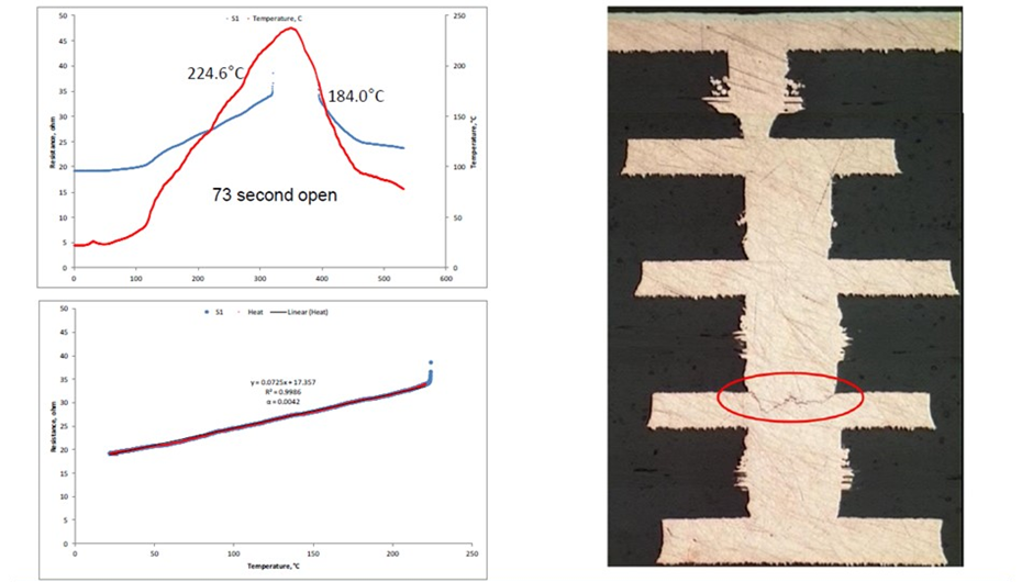
FIGURE 3. Reflow profile and 4-wire resistance of a 4+N+4 stacked microvia structure opening at only 224.6C and closing at 184C on cooling down. Subsequent room temperature testing and thermal cycling testing indicated no defect. [used with permission] [4]

 • Although the committee developed an FMEA for microvia defects, only this one WMI is our focus.
• Additional work by the committee or industry is needed to identify the root cause(s) and implement corrective actions. Volunteer’s for this committee are accepted provided they come to work. (contact Chris Jorgensen at IPC or Michael Carano at rbpchemical.net)
• Any industry data pertaining to this problem can be contributed to the IPC and will be used ‘anonymously’.

To further read about the WMI Committee and our findings, there is a report available from our APEX 2019 WMI OPEN FORUM[2] and a White Paper was published by the committee, IPC WP-023 “Via Chain Continuity Reflow Test: The Hidden Reliability Threat- Weak Microvia Interface.” Available from the IPC Bookstore.
Further discussions will be undertaken at the upcoming IPC Annual High-Reliability Forum to be held in Baltimore on May 14~16 [3]

REFERENCES
1. IPC Press Release, Mar 6, 2019
2. Weak Microvia Interface Open Forum, IPC APEX, Jan 2019, San Diego, CA
3. IPC High-Reliability Forum in Baltimore, MD on May 14-16, 2019
4. J.R. Strickland & Jerry Magera, How MSI Applied Technology Beat the Microvia Hidden Threat, IPC High-Reliability Forum, May 16, 2018, Baltimore, MD

 
  Go back to Contents


Section 4 Process Improvement Strategies for Weak Microvia Interfaces

William Bowerman, Jordan Kologe, Rich Bellemare and Warren Kenzie MacDermid Alpha Electronics Solutions
Waterbury, Connecticut, USA

 bill bowerman

Bill Bowerman
MacDermid Alpha

Abstract
The industry has been openly discussing the concern about weak microvia interfaces after IR reflow and the potential for an undetected open or latent defect that can escape after expensive components have been soldered to the board. A specific concern is for the reliability of stacked microvia designs on very complex panels that are often built in low volumes. This type of build is typical of American and European OEMs who are using large and expensive BGA components in mission critical electronics. Due to the limited number of units made, this board segment of the industry is more vulnerable to weak interface failure than the HDI boards for mobile devices that are made with high levels of automation in mass production by fabricators in Asia. Further complicating the board design impact, the metallization process that is used can have very different reliability performance from different lines in different regions.

The goal for the metallization process is to form a continuous metallurgical structure to withstand the thermo-mechanical stress of IR reflow during assembly. The best condition consists of epitaxial growth of a thin electroless copper deposit on the target pad with a grain structure that recrystallizes with temperature and becomes indistinguishable from the target pad and electrolytic copper structures. There are multiple factors that influence the ability to form this recrystallized structure, which in turn affects the strength of the microvia interface. These include the circuit design, laminate material selection, type and settings of laser via formation, post-laser conditioning of the target pad copper, the desmear and electroless copper process processes, and the electrolytic copper via fill plating processes.

Through extensive auditing as a supplier of primary metallization and electrolytic copper via fill chemistries, and cooperative work with PCB fabricator customers to improve microvia reliability, a wide range of studies were conducted. Presented in this paper are potential areas of concern for microvia reliability with a specific focus on metallization processes and the factors stated above as well as testing on improvements. The approach taken includes low level DOE testing for process improvement as measured by a test panel using IPC TM-650 2.6.26A and TM-650 2.6.27, otherwise known as IST and simulated IR reflow testing. Experience in failure analysis techniques, limitations on some commonly utilized inspection methods, and a review of overall best practices for plating are also discussed.

Testing was augmented with SEM, FIB, and broad-beam Ion Milling techniques to evaluate various the various structures. Current induced or air to air thermal cycling were utilized to determine the level of microvia survivability and judge process improvements.

Introduction
The goal of the electroless copper seed layer for primary metallization is to render the entire microvia surface conductive for electrolytic copper filling and to ultimately form a continuous metallurgical structure between the via target pad and the electrolytic copper plated with the via filling process. A well-formed microvia interface is thought to have the best resistance against interfacial separation caused by the thermal mechanical stress induced by reflow temperatures. Testing and screening for separation has been performed by Simulated IR Reflow in an air to air environment and by Current Induced Thermal Cycling above the Tg of the laminate where CTE mismatch is at its greatest.1,2 Both methods are useful for studying the robustness of the manufacturing process of HDI interconnects. Much of the North American and European HDI market is focused on aerospace, defense, and telecommunications electronics which design complex conventional HDI boards. To define conventional HDI, this paper will assume a core multilayer with 1 to several layers of HDI that can be stacked or staggered over buried vias. Stacked via structures that are greater than 2 layers have proven to be one of the greatest challenges to microvia reliability.

Other aspects critical to the survivability of the microvia interface through reflow not discussed in this paper include overall panel design, materials, lay-up, cure, via size and depth. Other authors have made contributions to understanding these topics.3 The focus of this paper is to offer some insight into the variety of conditions observed and best practices for metallization of microvias.

Via Formation and Target Pad Preparation
The importance of proper via formation and target pad copper preparation is critical to the interfacial bond. Laser via formation can have dramatic effects on the condition of the target pad. It can damage the target pad copper, leaving the surface coated with overly rough, loosely adherent and porous recast copper, or with a thin resinous layer of dielectric. Via formation is typically accomplished with two types of lasers: UV and CO2.

UV Nd:YAG lasers remove both copper and resin/glass material by high resolution photon ablation. The via is formed by the UV laser beam of ~ 20 µm (0.0009”) in diameter and smaller than the finished via. The laser beam has a short wavelength of 1,064 nm with a short pulse duration of ~120 ns and a pulse rate of 10 KHz. The tool has several options to control the path of the laser spot to form the required diameter microvia. The energy of the laser must be matched to the thickness of the copper and dielectric material as the UV laser does not inherently stop at the target pad during the drilling process. If the energy is too strong, the target copper can be plowed becoming overly rough with the ablated copper re-condensing on the surface creating what is known as recast copper. This recast copper is loosely adherent with an amorphous structure that will weaken the microvia target pad interface. The recast copper can cause a porous electroless copper deposition susceptible to hydrogen gas entrapment. The UV laser can be programmed with a defocused beam as a cleaning step to remove remaining resinous debris and maintain a smoother copper topography. Figure 1 shows progressive photos of a UV lasered microvia after UV cleaning, plasma cleaning, and one to two chemical desmear passes as well as the topography of recast copper from a top-down and cross-sectional view.


Fig 1
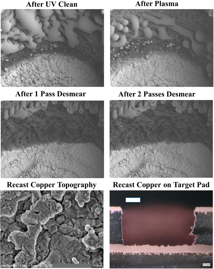
Figure 1 – UV drilled microvias shown after defocused laser clean, plasma clean, and 1x-2x desmear, recast copper macro-rough topography on un-plated target pad.


CO2 lasers remove resin/glass by low resolution thermal ablation. The CO2 laser has a long wavelength of 10,600 nm, with a pulse duration of µs and a larger beam diameter of 40 – 75 µm that can be reduced to a focal point by lenses and apertures.
The CO2 beam reflects off copper. In the past, a conformal mask or capture pad was etched followed by the CO2 laser to remove resin/glass in the dielectric. Today, with the use of thinner copper foils and Laser Direct Drill (LDD) oxide coatings, the energy of the CO2 laser can be absorbed by the copper and the beam can machine through the capture pad copper. While the CO2 beam will inherently stop at the target pad copper, one drawback is that as the CO2 beams nears the target pad, ~ 0.1 µm (4 µ”) from the surface, the energy is absorbed by the underlying copper and a thin resinous layer is left at the bottom of the microvia.4 This thin layer is removed by either plasma, chemical desmear or a combination of both.

Combination UV-CO2 lasers have rapidly become the tool of choice in North America and Europe for HDI via formation. The UV laser beam first removes the copper from the capture pad, as well as some of the resin/glass below, defining the opening. The CO2 laser beam then removes the remaining resin/glass material down to the target pad. Both the UV and CO2 lasers create heat that melt the glass and leave carbonized debris on the side walls. The UV beam is again used but defocused, providing an optional cleaning step to remove the residual film without damaging the target pad. Figure 2 shows the appearance of a microvia drilled with a combination UV-CO2 laser after laser, plasma, and desmear passes.

Recently, pico-lasers have also been introduced for via laser formation. The pulse duration for these lasers is in picoseconds, which significantly reduces the amount of heat damage to the resin/glass and copper. The result is little to no heat affected zone in the via wall or the target pad. Pico lasers are also known as green or cold lasers.

Based on the laser tool used and the condition of the microvia wall and target pad, the fabricator may incorporate several cleaning steps prior to metallization. These include a pre-etch, plasma and chemical desmear.

 Fig 2

Figure 2 – UV-CO2 laser drilled microvias shown after shown after UV clean, plasma, and desmear.


Chemical Cleaning
Horizontal pre-etches are widely used in HDI mass production. The pre-etch removes 0.5 to 1.0 micron (20-40 µ”) of copper per pass with two passes with a flip in between being common. Pre-etch lines utilize spray bar modules similar to copper reduction designed for a high degree of etch uniformity across the panel surface. Hydrogen peroxide etchants are most common, but persulfate etchants are suitable as well. The pre-etch removes recast copper, excessive roughness and may undercut and remove some remaining resinous debris, as can be seen in Figure 3.

Fig 3
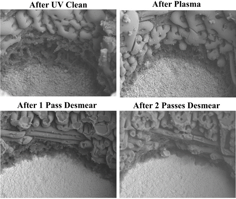
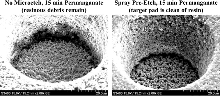
Figure 3 – The effect of chemical pre-etch on resinous debris.


Chemical desmear acts as the main microvia cleaning step. Plasma and desmear can be used in combination depending on the laminate material and plasma capacity at the fabricator’s facility. Fortunately, chemical desmear is the same process used for through-holes and can be run horizontally or vertically. Most horizontal lines will run desmear twice, flipping panels between runs. Vertical lines can also run HDI panels twice by programing the hoist movements. The chemical desmear process includes a solvent swell, sodium permanganate and a neutralizer. Sodium permanganate is utilized due to its high solubility that prevents flash drying within the microvia during drip time and transfer. Either a non-etching neutralizer or a sulfuric peroxide etching neutralizer may be used. Etching neutralizers are balanced to etch a minimum amount of copper. A glass frost (1-3 g/L) or glass etch (>55 g/L) can also be included in the neutralizer bath or in a separate step.

A 2 level DOE test comparing type of UV-CO2 Laser, 2X and 4X desmear cycles, and with / without flash plating was conducted. The response was failure rate in simulated IR reflow, specifically the lower the mean failure rate of 50X reflow cycles, the better as shown in Figure 4. The Pareto chart in Figure 4 shows the interaction of the desmear and UV clean as significant in improving reliability. The defocused UV clean and extra cycles of desmear had the lowest mean rate of failure. It was also determined that the use of flash plating or simply going directly into copper via filling without flash plating was not significant in this study.

Fig 4

 Figure 4 – 2 Level DOE results for UV clean, desmear cycle, and flash plating impact on 50x reflow failure rate.


Best Practices for Electroless Copper Deposition
It has been determined that the electroless copper grain structure type is critical to microvia reliability. Over a two-year time span of global auditing of desmear-electroless copper lines with the goal of increasing process robustness and improving microvia interface, a set of best practices for maintaining good electroless copper grain structure have been determined. The desmear process is followed by the electroless copper metallization. Most desmear/electroless copper lines will run together with the panels going wet to wet. This is the preferred sequence. If this is not the case, it has been determined that the Cleaner/Conditioner on the electroless copper line should utilize either ultrasonics (horizontal lines) or vibration and thump (vertical lines) to de-gas microvias and wet all surfaces quickly and uniformly. With thousands of microvias on a typical HDI panel surface, a single gas bubble can ruin a panel. Furthermore, it is recommended that vertical lines are equipped with vibration capability for all process tanks in addition to the cleaner/conditioner.

A dense, angular electroless copper grain structure is preferred with a strong, 1, 1, 1 oriented, face centered cubic crystal structure. 1,1,1 is the densest atomic packing of copper atoms with the lowest total energy state. Grain structure can be evaluated with a simple top-down comparison using SEM imaging at 1,000X and 5,000X of the surface copper and target pad copper. Both grain structures should look similar. It was found that controlling the grain structure required good solution exchange into the microvia and maintenance of the concentration of the primary grain refiner agent in the bath. Electroless copper grain refiners work by temporary adsorbing on the cupric ions at the surface during plating, increasing the activation energy and causing a two-step reduction process from cupric+2 to cuprous+1 to copper. Grain refiner components are typically easy to analyze and most commercial electroless copper formulations maintain an adequate concentration with normal bath replenishment.

It was also found that chemical exchange into the microvia is important to obtain the desired grain structure at the target pad. Because of the shape of the blind microvia structure, achieving proper solution exchange is more difficult than in open through holes. The main reactants in the electroless copper reaction are diffusion controlled so the exchange to the bottom of the via is critical. Copper ions, sodium hydroxide, and the methylene glycol ion (formaldehyde reducing agent) are smaller ions in g/L quantities. The stabilizers and grain refiners are larger ions and are in ppm and ppb levels. These components are diffusion controlled. Solution exchange is critical to maintain all components during the initiation and autocatalytic phases of electroless plating. A 2 level DOE was run to investigate the influence of panel location in the rack, specific gravity, grain refiner concentration, vibration and air agitation. The response was the grain structure of the target pads at 1,000X and 5,000X SEM images using a rating on a scale of 1 – 5 (higher is better). Figure 5 displays a summary of the results of this study. The grain refiner concentration, specific gravity, vibration, and location on the panel rack were found to be significant factors in the quality of the electroless copper plated at the target pad.

Fig 5

Figure 5 – Top, main effects plot for solution movement DOE. Bottom, copper grain structure at base of target pad rating system examples.


Panel racking is an important factor for solution exchange in microvias in HDI processing. Racks should hold panels 90o vertically to not favor either side, differing from the way through-hole only panels would be processed in an angled configuration in earlier PCB manufacturing. Vibration is run on an on/off cycle to increase solution exchange in the microvias and dislodge hydrogen gas bubbles generated during electroless copper plating. From a chemical reactant standpoint, two moles of hydrogen will evolve for every mole of copper plated, so the gas removal is an important factor to control and understand. An accelerometer can be used to check the vibration energy level. 4 mm/s is recommended. The rack must secure the panels tightly to ensure transfer the energy to the panels completely and in a repeatable manner.

General bath solution movement also plays a role on grain structure development. It was found that panels racked on the outside of the basket saw more solution movement than those racked on the inside giving the outside panels a more desirable grain structure at the microvia target pads. In horizontal lines, it is easier for hydrogen gas to escape on the top of the panel versus the bottom of the panel, which also complicates solution exchange and hydrogen gas bubble removal during plating. This can be remedied by the usage of multiple fluid bars to help remove the trapped gas.

It was found that aspect ratio of the microvia structure also has an influence on electroless copper grain structure at the target pad. A study was conducted with 7 different via diameters drilled on one panel. The dielectric on one side was 3.5 mils and
5.5 mils on the other side giving aspect ratios of 0.35, 0.44, 0.60, 0.78, 0.88, 0.93 and 1.13. Grain structure was evaluated on a scale of 1 – 5 (higher is better). It was found that the microvias with aspect ratios of 0.75 and lower allowed for good solution transfer and better electroless copper grain structure at the target pad area. As the aspect ratio increases to 1 and greater, the transfer of solution declined and the grain structure deteriorated. This can be seen in Figure 6, which shows the results of the study. In all, it is hypothesized that the variation in grain structure is related to the solution transfer since higher aspect ratio vias have an increased diffusion layer, which reduces the PPM level of the grain refiners that are utilized in the formation of the deposit.

Fig 6

Figure 6 – Top: Experimental results that display the effect on microvia aspect ratio and diameter on grain structure quality. Bottom: Example of plated electroless copper at the via target pad and the rating of grain structure.


If the pitch and target pad diameter of the design allow for it, a slightly larger diameter microvia can be beneficial to the robustness of the via interface. This is limited by via filling chemistry however, as current copper micro via filling processes cannot effectively fill vias wider than 150 microns (6 mils) in diameter with a flat surface or less than 5-micron dimple.

Rinsing is an often-overlooked step in the metallization process. Several troubleshooting efforts undertaken during the auditing study have found poor rinsing to be causal to microvia separation or microcrack starts. The separations might not be catastrophic or occurring on the first reflow cycle but can result in a shortened number of reflow cycles or show up as partial or starter cracks near the wedge area during examination. Rinse water contamination has often found to be the main contributor to microvia failure, even more so than rinse time. Contamination of rinse water is one of the most difficult causes to pin down as review of the process when troubleshooting will show no issue associated with the rinsing time, and any water contamination that may have caused the defect will often no longer be present by the time the defect is found. Other areas of concern for rinsing include the wetting agents that are included in the cleaners, and the impact that these may have on the effectiveness of the activation process. In auditing the lines, it was found that treating every tank as a separate process to control on its own allowed insight on previously unexamined factors that impact the robustness of the microvia target pad interface.

Through a study of a specific board build that experienced pad separation before reaching the required 1,000 cycles in IST testing it was found that the specific gravity of the electroless copper bath was a significant factor. Lowering the specific gravity by 0.2 units from the maximum specific gravity on as identified by the commercial technical data sheet for the process helped mitigate the separation problem and allowed the IST test to run to the censor point. Through this study it was determined that for running HDI panels, suppliers of commercial electroless coppers should recommend that the specific gravity of the bath should be slightly below the maximum level compared to that of through-hole only builds. It is hypothesized that the higher level of by-products, formate and carbonate species, are competing with the main reactants at the diffusion layer as shown in the earlier study as a significant interaction. The results of this study can be seen in Figure 7 below.

Fig 7

Figure 7 – Study: Adjustment of the control levels for the specific gravity of the electroless copper bath for HDI.

A study was done, selecting panels run at various sites around the world to see the effect the grain structure had on simulated reflow testing per IPC 2.6.27. Figure 8 shows the electroless copper grain structure at the via target pad for the various sites A-E. The same electroless copper formulation was run at different sites for A, B, C and D. Site E was a different electroless copper formulation. Sites A and B show the ideal angular grain structure. Sites C and D show a dense structure but not ideal. Site E appeared porous and cauliflower like. Sites A and B passed 24 OM cycles as the censor point while the other panels had some level of failures before 24 cycles.

Fig 8

Figure 8– Electroless copper grain structure plated at various sites around the world.


Epitaxial Grain Growth
Epitaxial copper growth is important for both electroless and electrolytic copper plating. Epitaxy refers to the ordered crystal growth over the substrate copper, wherein the case of electroless copper plating in the microvia, the deposition will mimic the parent target pad copper.5 The quality of the substrate copper is the reason for this paper’s earlier discussion of the laser via formation and pre-etch steps as removal of unwanted recast copper and excessively rough copper is an important factor to proper grain growth.

To achieve an epitaxial copper structure, the initial copper deposit needs to mirror the substrate crystal structure. If the target pad has recast copper, the structure is amorphous and the resulting target pad interface will be weak. If the target pad is too rough, the electroless copper solution will be in contact with too many crystal facets to grow uniformly possibly resulting in a porous coating with nodules. It was found that the ideal surface roughness for the target pad after micro-etching is between 0.4 and 0.5 µm Ra or 0.15 and 0.20 µm RSAR. A persulfate or sulfuric peroxide etch on the copper will provide topography in this range, with the persulfate being more matte and the peroxide less so. A study was conducted that examined how the roughness of the base copper changed after mono potassium persulfate (KPS), sodium persulfate (SPS), and sulfuric-peroxide etches (H2SO4/H2O2), and the appearance of the subsequent electroless copper plating grain structure over the various etches. It was found that the electroless copper deposited over the micro roughened base copper will replicate the topography. The details of this study can be seen in Figure 9 below.

Fig 9

Figure 9 – Etch chemistry impact on roughness and topography of the underlying substrate.


Thickness of the electroless copper deposit is another factor to be considered. Both thin dep, ~ 0.3-0.5 µm (12 – 20 µ”), followed by an electrolytic copper flash or medium dep, 0.8-1.25 µm (32-50 µ”), have track records of being reliable. The copper deposits will form an identical structure over the substrate copper. Heavier deposits of 2-2.5 µm (80-100µ”) are not recommended for HDI. It should be noted some electroless copper baths will plate less copper on copper than on epoxy dielectrics. This is considered a favourable characteristic allowing for good coverage of the dielectric in the via wall while keeping the copper deposit on the copper land thinner.


Electrolytic Copper Via Fill Guidelines
Electrolytic copper via fill follows the electroless copper seed layer in crystal shape.6 The goal is to continue the grain orientation in the 1,1,1 crystal plane. If the target pad and seed electroless copper have followed the epitaxial crystal structure, the electrolytic copper will follow the same crystal orientation. For conventional HDI panels, pattern or button plating are common. Microvias are plated first, followed by a second pattern plating cycle for through holes. Today there are commercial chemistries available for simultaneous via fill and through hole plating with the through hole aspect ratios limited to approximately 6:1.

Panel plating is utilized for Any layer HDI designs which have no through-hole plating. The panels are processed from the electroless copper directly to copper via fill without the imaging step in-between. This less complex metallization cycle is mainly used in mobile applications and is the largest segment of HDI globally.

Electroless copper lines with low dep thickness will typically be followed by an in-line flash. This is important to protect the thin dep copper during imaging and pre-cleaning for plating. In-line flash plating is ideal to prevent the formation of oxides on the copper surface. If the lines are not connected wet to wet, then the panels should be held for a limited time in dilute sulfuric acid or coated with an anti-tarnish.

Some lines for copper via fill chemistry start with an acid cleaner and light microetch while others have an in-line flash plate. Re-activating the copper surface after dry film development and rinse is important to have uniform plating without dimples. A dilute persulfate microetch of 0.1-0.2 µm (5-8 µ”) is recommended. The sulfuric pre-dip before plating should be changed to prevent the build up of copper. Copper concentrations over 200 mg/L have been found to degrade reflow survivability.

Copper via fill current densities should follow the supplier’s recommendations. A multiple step current density ramp is often used with lower current density to promote bottom up fill and then increase the current density for productivity. On plating lines with direct impingement, the flow rates can also be adjusted. A high flow is used in the beginning to promote bottom up plating but then the flow rate is lowered so the plating height is uniform without dimple.


Copper Recrystallization Across the Interface
If best practices have been maintained over the metallization process sequence, the plated copper will undergo grain growth under time and temperature.7 During this self-annealing, the crystal structure coarsens to reduce grain boundaries. A study8 of this phenomenon utilizing cross sectioning and FIB (Focused Ion Beam) and IM (Ion Milling) SEM imaging showed a continuous structure across the three interfaces when proper metallization process guidelines were maintained. Figure 10 below shows an IST coupon with 3+N+3 stacked vias over a filled buried via, which is one of the types of designs that has shown concern for microvia reliability. The coupon was run 9 times in IR reflow at 260oC followed by 1,000 cycles of IST. After the thermal-mechanical stresses of the test, the electroless copper deposit could not be detected in the FIB image.

Fig 10
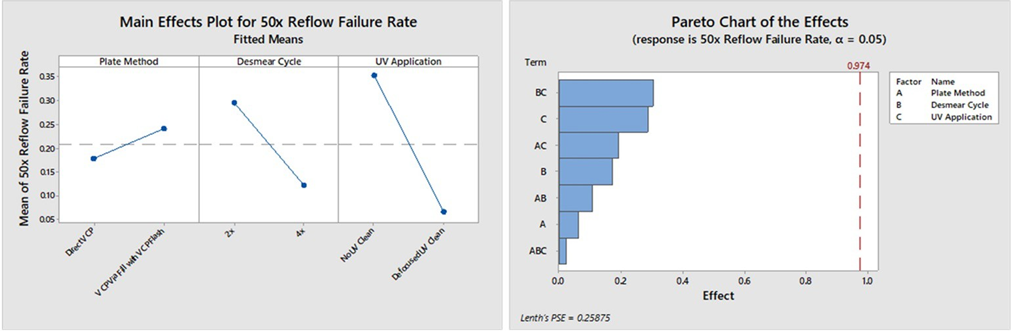
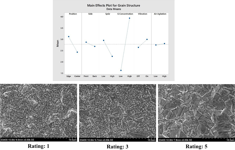
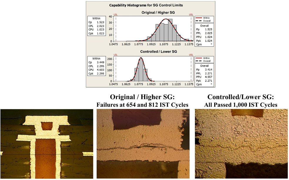
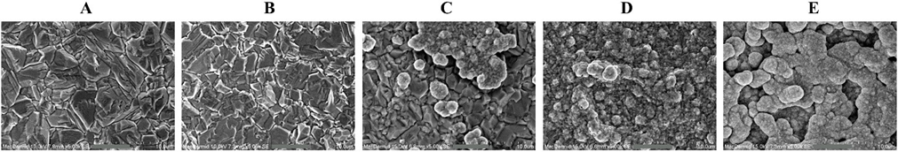
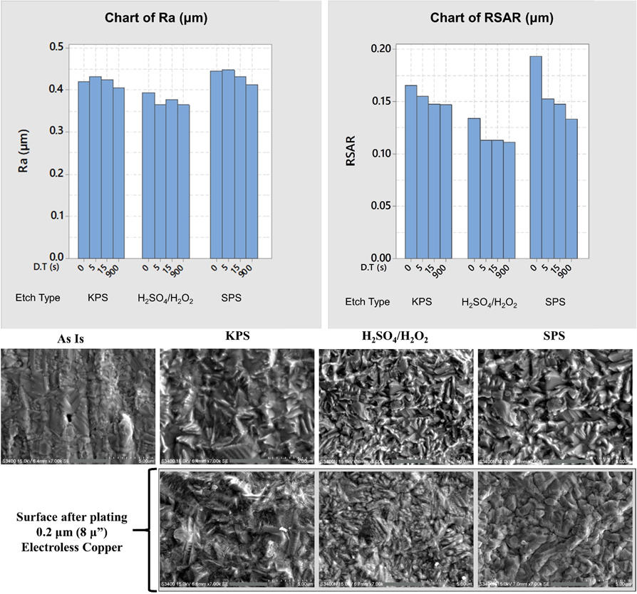
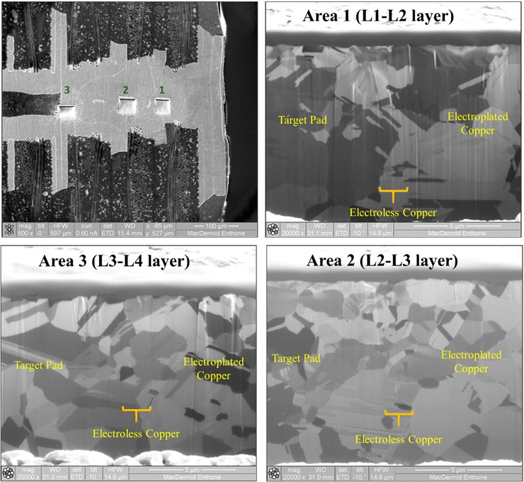
Figure 10 – 3+N+3 Stacked microvias showing continuous grain structure and strong layer to layer bonding.

Recrystallization had formed a continuous grain structure indicating strong layer to layer bonding. Lack of recrystallization across the various copper interfaces can be attributed to several factors. Recrystallization can be interrupted by a macro-rough surface on the target pad, from recast copper, from a layer of oxidization on any interface during metallization, dry film or developing residues, or by a non-epitaxial copper structure that did not follow the orientation of the substrate.
Recrystallization may not have occurred uniformly across the interface leaving a weakened interface. A porous or cauliflower electroless copper deposit may leave hydrogen entrapment or nanovoids in the layer.


Summary and Conclusions
The microvia has been the primary enabler of high-density interconnect since its inception but concerns over weak via target pad interfaces have so far limited the usage of this design feature in devices that require very high reliability. As HDI designs are becoming more widely utilized in mission-critical and safety-oriented applications, the focus on solving the issues behind the weak microvia interface has never been more important. Continued studies such as the ones presented in brief in this review are necessary to facilitate the next step in high reliability design. Important areas to focus on are the condition of the copper at the target pad before plating begins including the presence of recast copper, surface roughness, selection of laser equipment, and chemical etching treatments. These factors have a large impact on the topography and grain structure of the subsequent electroless copper deposit and are critical to achieving the uniform recrystallization required to have a sound target pad interface. Additional factors discussed such as rinsing, electroless copper grain refiner concentration, solution movement, panel racking and control of hydrogen gas during plating of copper are important and should be maintained according to best practices to achieve reliable results.
References
[1] IPC-WP-023, The Hidden Reliability Threat – Weak Microvia Interface, Jerry Magera, MSI, May 2018
[2] The Keys to 100% Effective Reliability Testing and Failure Analysis of HDI/Microvias, Kevin Knadle, IPC High-Reliability and Microvia Summit, May 2019, S16-03
[3] Microvias: Links of Faith Are Not Created Equally, Jerry Magera, IPC Expo 2021
[4] Studies on CO2 Laser Drilling: Formation Mechanism of Residual Thin Materials at the Bottom of Laser Via, Ryoji Inaba, and others, Hitachi Via Mechanics, IEEE, Vol 24, No 1 January 2001
[5] Microstructure Evolution during Electroless Copper Deposition, J. Kim, IBM Res Develop, Vol 28, Nov 1984
[6] Substrate effect on electrodeposited copper morphology and crystal shapes, Swastika Banthia, Surface Engineering, 2018, Vol 34
[7] Crystallographic study on self-annealing of electroplated copper at room temperature, Eri Shinada, Mat’l Sci in Semiconductor Processing, 16 (2013)
[8] Time Evolution of Stress and Microstructure in Electroless Copper Films, Tanu Sharma, Electrochimica Acta, 196 (2016)

 
  Go back to Contents


Section 5

Ultra Thin Base Materials Take PCB Manufacturing to the Next Level

Daniel Schulze
Dyconex

 schulzeDaniel Schulze
Application Engineering Manager - Dyconex 

Almost all markets are experiencing increasing demand for smaller and thinner electronic devices. Today’s mobile devices are small enough to fit in a watch, and the aerospace and automotive industries desire smaller and lighter devices to lower fuel costs and reduce emissions. Likewise, the medical industry needs wearable sensors, implantable devices, and handheld instruments that are small and lightweight.

Manufacturers of the printed circuit boards (PCBs) that are at the heart of these electronic devices have been making them more compact and lighter primarily by decreasing the size of the copper features and board materials. Extremely thin base materials are making it possible to take miniaturization beyond what was previously possible without compromising reliability or performance.

Thinner Substrates
Although a great deal of miniaturization can be achieved in the X and Y directions, the technology is beginning to reach its limits. Another level of compactness is possible by using rigid and flexible ultra-thin base materials to make highly reliable PCBs that are thinner. While miniaturization in X / Y direction can greatly reduce the footprint of PCBs, miniaturization in the Z direction leaves more space for other components and reduces the overall thickness of the device.

pacemaker evolution

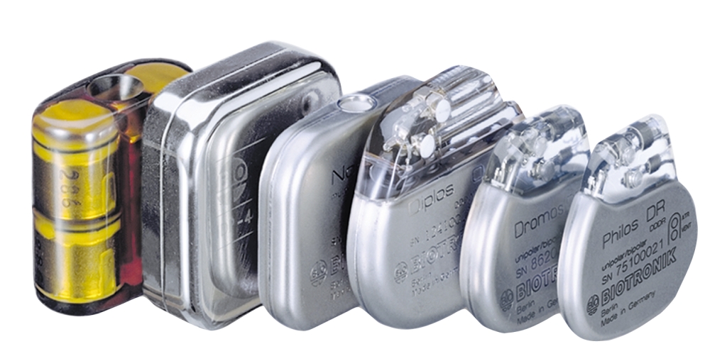
Figure 1. Evolution of pacemakers. Image courtesy of Biotronik.

With thinner base materials, less plated copper is needed to fill via connections. This automatically results in thinner copper layers and, therefore, lines/spaces with smaller resolutions and a reduced interconnect footprint.

Flex systems
Medical devices, like hearing aids and active implants, often require PCBs that can fit into the smallest area possible to improve the patients’ comfort. With flexible substrates, it is possible to create PCBs that fold to reduce the surface area and volume needed to house the PCB and thus increase the integration density. Using thinner flex materials rather than traditional thick flex materials can reduce the space needed for the PCB even more. For example, a six-layer flex system is about half the thickness of a system fabricated with standard flexible materials.

6 layer stack

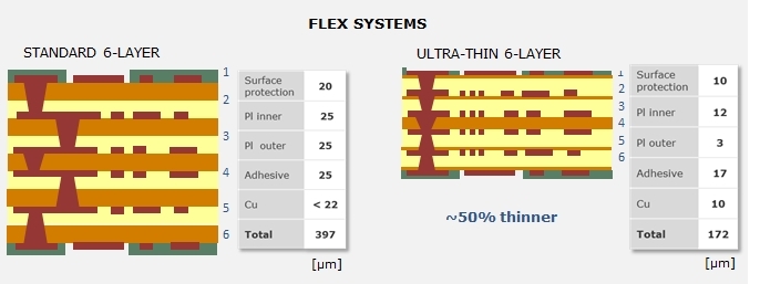
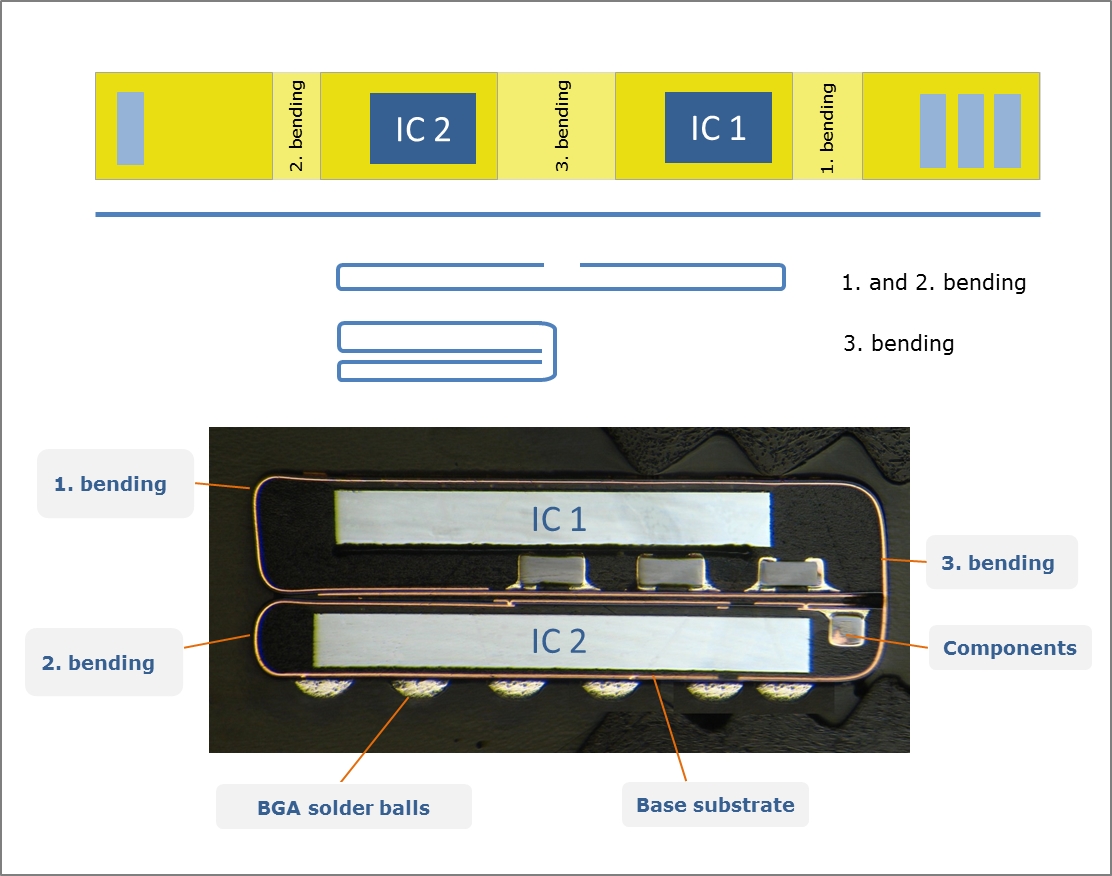
Figure 2. 6-layer stack-up with standard flex material compared to 6-layer stack-up with ultra-thin base material.

Flex systems are used in hearing aids to ensure all the necessary electrical components can be housed within a package that fits in the ear canal. In this case, the circuit board is assembled flat with the integrated circuits, resistors, and capacitors and then folded to reduce the overall footprint.

folded packaging

Figure 3. From flat substrate to folded package.

Ultra-thin flexible substrates also allow better bending. This means the PCBs can be bent with smaller bend radii to achieve even smaller volumes. A comparison is shown in Table 1. The improved bending makes ultra-thin flexible materials ideal for making cables that require dynamic bending, as in robotic arms.

   Total Thickness  Min Bend Radius
 Standard 6-layer  397 µm  2.38 mm
 Ultra-thin 6-layer  172 µm  1.03 mm

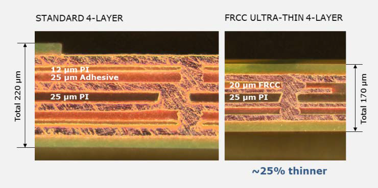
Table 1. Comparison of minimum bend radii according to IPC-2223 5.2.4
(6x total thickness PCB).

Today, the outer layers of a multilayer flex system typically measure 12 µm for the polyimide and 12 µm for the adhesive. The new Flexible Resin Coated Copper (FRCC) material available offers 3 or 5µm thick polyimide outer layers combined with a minimum 17 µm thick adhesive layer. 

cu clad polyimide    Thickness (µm)
 Copper  12
 Polymide (PI)  3, 5
Adhesive (Adh) 17, 20, 25, 28

 Figure 4. Cu clad polyimide laminate.


 Properties  Unit Pi ADH
 Dielectric constant (1 GHz) --  3.3 3.0
 Dissipation factor (1 GHz) -- 0.01  0.019
Surface resistivity MΩ  3x10⁸  
 Volume resistivity  1x10⁸ Ω*cm  1x10⁸  
Insulation resistance MΩ 1x10³  MΩ  1x10³  
Dielectric strength  kV/mil  2 n/a
Peel strength (initial/aging)   kN/m 0.8  
Youngs modulus GPa 4 1
CTE (XY) ppm/K 25 80, 580
CTE (Z) ppm/K n/a 210
Glass transition temp. Tg (DMA) °C 320 70, 210
Moisture absorption (23°C, 24h) % 1.0
Flammability -- VTM-0

Table 2. Characteristics of FRCC materials.

 4 layer flex

 Figure 5. Standard 4-layer flex system vs. ultra-thin 4-layer flex system
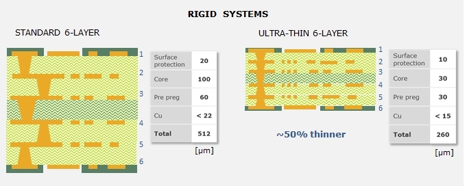
 

Rigid Systems
For applications that require a 2D PCB, ultra-thin rigid materials are available. These are typically used as packaging substrates for ICs, where they help make the entire component very thin. For example, a 6-layer rigid system using an ultra-thin material is about 260 µm thick, the same system with standard material is 512 microns thick. With the ultra-thin rigid materials, it is possible to achieve pitches smaller than 175 microns, lines or spaces 25 microns wide, via diameters of 50 microns, and pad diameters of 100 microns.

 6 layer rigid

Figure 6. 6-layer stack-up with standard rigid material compared to 6-layer stack-up with ultra-thin base material.

  Standard Material  Ultra-thin Material 
Thickness of rigid 6-layer system  512 µm 260 µm 
 Lines / Spaces  50 – 70 µm 30 – 50 µm 
Via diameter   75 µm  50 µm
Pad diameter  150 µm  100 µm 
 Pitch 250 µm 175 µm

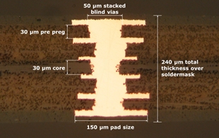
Table 3. Comparison of design features for 6-layer systems

 6 layer via hole

Figure 7. 6-layer rigid stack-up with ultra-thin materials.

The coefficient of thermal expansion of the rigid substrate is one of the most important properties for chip packaging substrates. If it is not matched well with the silicon die, it can lead to cracks that adversely affect packaging production and the assembly of the components onto the substrate. Problems with thermal expansion can even lead to failures during device use. Ultra-thin substrate materials also need to have very good high-frequency properties to achieve the requirements of today’s high-speed telecom applications.

 Properties Unit Conditions Value
 CTE

ppm/°C
 ppm/°C

XY < Tg
Z < Tg
 5-6
18-22
 Tg °C  DMA  280-300 
 Flexural modulus Gpa  25°C   32
 Dielectric constant 𝜀𝑟
𝜀𝑟
1 GHz
10GHz 
4.4
4.3 
 Dissipation factor - -
- -
 1 GHz
10GHz 
0.006
0.008 
Dielectric strength  Kv/mm ASTM D149
Method A 
103
 Moisture absorption %   0.3 
Min thickness core µm   30
Min thickness pre-preg µm   20

Table 4. Characteristics of advanced ultra-thin rigid material.


Considerations for Ultra-Thin Materials
Because ultra-thin materials require specific design approaches, fabrication technology, and other considerations, it is critical to use an experienced PCB manufacturer with advanced engineering services.

Advanced techniques such as laser direct imaging can be used with ultra-thin materials, but highly precise registration processes are required because the features are typically smaller when a thinner material is used.

It’s important to note that the thinner material can lead to warpage and increased flexibility, which make proper handling during assembly more critical than with traditional materials. The reduced dimensions and smaller pads require higher accuracy during assembly, and when thinner materials are used, it can also be more difficult to place the finalized circuits into the end application without breaking them. Because of these challenges, it is critical to have early discussions with the PCB manufacturer regarding handling requirements and the number of units within a delivery panel.

The additional handling and fixtures needed with ultra-thin flex materials increase assembly and handling costs. However, lower process and material costs can help balance these. Material costs are reduced as less copper is required. Consulting with the engineering team of the PCB manufacturer during the design phase can help ensure the most cost-effective solution that meets the performance needs of the specific application.

Assuring Quality and Reliability
The reliability of the interconnect structure improves with thinner stack-ups when using ultra-thin materials. Smaller expansion along the Z axis results in less stress for vias during temperature cycles.

Dyconex has created a center of competence for product reliability. This testing laboratory unifies all the processes necessary for precise monitoring of product reliability. The equipment includes stations for electrical fault isolation and thermography as well as multiple interconnect stress test (IST) units, bending testers, a soldering simulation oven, and instruments for thermomechanical and dynamic mechanical analysis (TMA, DMA). Furthermore, a scanning electron microscope and various optical microscopes can be used for investigations.

For critical medical or aerospace applications, the laboratory has developed extensive and systematic methodologies that make it possible to gather solid evidence about product reliability by employing accelerated test procedures such as the IST test. In IST tests, special test coupons that include vias are subjected to temperature cycles, after which they are measured for possible changes in resistance within the test coupon. Any corresponding increase in resistance is indicative of damage.

Conclusion
Ultra-thin PCB base materials are suitable for all markets where miniaturization and high reliability play a role. They can enable miniaturization with increased functionality through higher-density designs. Thinner material leads to smaller vias, reduced aspect ratio of vias, smaller lines and spaces, less copper plating, and better fill grades, but it can also increase handling complexity. Working with a PCB manufacturer that offers advanced engineering services can help ensure your design is compact while remaining cost-effective and reliable.

Daniel Schulze has studied at the Technical University of Dresden and holds a diploma in electrical engineering. During his diploma thesis and an internship at the Georgia Tech Packaging Research Centre, he got involved with working on optical waveguides embedded in PCBs. In 2005, he began as product engineer at Dyconex AG. Since 2008, he has been an engineering manager at Dyconex and is responsible for the product development of PCBs used in medical imaging, hearing aids, cochlear implants, industrial, and HF applications.

 
  Go back to Contents


Section 6

Computer Aided Engineering Simulation for Production Proofing PCB Copper Plating

Robrecht Belis, Elsyca, Belgium


Robrecht Belis

 Robrecht Belis
Head of Sales
Elsyca, Belgium

Maximizing production yield is vital for PCB manufacturing.
As the PCB industry is coping with ongoing miniaturization, shorter delivery times, and profit margins that are increasingly under pressure, manufacturers need to deliver ever more complex and higher-quality boards at a lower cost. A significant factor affecting the cost of manufacturing PCBs is production yield. High-end PCBs stretch production processes to their limits, resulting in more out-of-spec products. Therefore, increasing production yield through better control of the different production steps is an absolute necessity for every PCB production manager. But as the outcome of the production process depends on the PCB design and the panel layout, increasing production yield can only be achieved through a joint effort of all PCB production stakeholders.

Copper plating processes have a profound impact on production yield.
The copper plating steps are among the most critical steps in the production of PCBs. To avoid significant quality and performance issues, PCBs need to meet a uniformity specification regarding finished copper thickness. Hence, the plating process needs to deposit a minimum amount of copper in all holes while, on the other hand, the surface of the board cannot be overplated. Prototyping and subsequent trial runs are time-consuming and expensive iterative methods for achieving this. A software tool to predict the outcome of the copper plating process proves to be a much more viable option.

Maximum uniformity of finished copper thickness is achievable only if designers and CAM engineers act on time.
Since designers and CAM engineers have no direct control over the copper plating process, they may feel there is little or nothing they can do to achieve a uniform finished copper thickness of PCB traces and holes.
Nothing could be further from the truth, however. Both board design and panel layout do have a massive impact on the finished copper layer thickness. By recognizing this impact, designers and CAM engineers can substantially increase the potential to uniformize the finished copper thickness as long as they act well ahead of committing PCB panels to production.

A novel CAE simulation technology empowers designers and CAM engineers to optimize PCB copper plating.
Notwithstanding the complexity of copper plating processes, Computer-Aided Engineering (CAE) simulation technology makes it straightforward for PCB designers and CAM engineers to quantify any unwanted variations of the finished copper thickness. Rather than making this optimization by a manual trial-and-error process, an auto-intelligent copper balancing approach is used. This approach makes it possible and practical for any PCB designer or CAM engineer to optimize PCB copper plating long before committing to production. They can provide process engineers with the best starting point and eliminate the need for expensive set-up changes during production (if such changes are possible at all).

The needs of Production
As soon as PCB panels are committed to production, the board design and panel layout are fixed, and any flaws that harm the copper thickness uniformity can no longer be undone. At this stage, it’s become far too late for any corrective measures on boards or panels. Hence, there is nothing else that process engineers can do but work on parameters that impact the uniformity of the electric field in the electroplating bath.

1. Putting PCB design right on track for manufacturing success
In the first step, simulation empowers PCB designers to get high-quality predictions of the finished copper layer thickness on a board design. Without the need for specialized knowledge, they can then quickly resolve any copper layer thickness issues in out-of-spec areas thanks to auto-intelligent copper balancing capabilities.
As a smart algorithm adds dummy copper features to the existing design and continues to check the impact on the copper layer distribution until it delivers an optimized result. By leveraging integration within ECAD environment, both the copper check and related optimization do not require any effort for PCB designers.
The obtained final design (including copper balancing areas) can be tested before being sent to the manufacturer. This ultimately avoids expensive and time-consuming re-spins. It does nothing less than put any PCB design right on track for manufacturing success.

2. Hitting a sweet spot between quality and cost
While PCB designers use simulation to uniformize the finished copper thickness on individual board designs, the thickness distribution can still change across circuit boards on a panel committed to production. To address that issue, CAM engineers can either resort to modifying the layout of the panel or apply smart copper balancing in-between the PCBs. The latter approach auto-updates the panel’s active copper fraction and provides process engineers with the best starting point for fine-tuning copper plating production settings. Here again, validation and related optimization can be integrated within existing CAM tools to ease CAM engineers’ work.
fig 2Starting from a graphical overview of the finished copper thickness distribution over the entire PCB panel, CAM engineers can easily assess any critical areas that remain and advise the production team which PCBs need testing and which areas these tests should focus on. That applies in particular to vias and through-holes, where the presence of a sufficient copper thickness is a critical quality indicator.

3. Fine-tuning production settings to deliver a top-quality PCB
Simulation enables process engineers to complete the work set in motion by designers and CAM engineers. Process engineers can run various what-if analyses on a digital twin of their in-house electroplating tank to examine feasible scenarios for mitigating local current density peak effects during the copper plating process.
What-if analyses typically validate the impact of layout modifications (like spacing between panels), tooling (like shields), or process parameter (like plating time or rectifier properties) changes. As such scenarios can be investigated in a matter of minutes, an optimized copper plating set-up can be achieved without any guesswork or expensive trials.

PCB Design

Finished thickness of copper traces and holes is critically important
The PCB design process defines a junction of copper traces that interconnect the components mounted on both sides of a circuit board. Along with their width, the thickness of these copper traces determines the amount of current the circuit can carry. As a result, the finished copper thickness of traces and holes (and its uniformity in particular) is critically important to the quality of a manufactured circuit board.
The manufactured product, therefore, needs to meet a uniformity specification regarding finished copper layer thickness.

 fig 5  fig 6

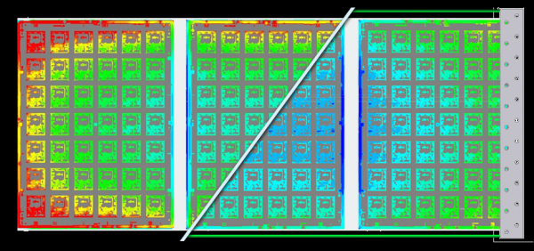
PCB Layout before and after copper balancing

(Right picture – black areas represent added dummy copper features)

Existing DFM tools do not allow to assess finished copper thickness
Rather than focusing only on the design process itself, PCB designers need to make sure circuit boards are designed in a way that makes it easy to manufacture a quality product. Hence, modern PCB design software includes the tools that help designers comply with Design for Manufacturability (DFM) rules and guidelines and deliver PCB layouts that facilitate manufacturing and assembly processes.
However, none of these DFM tools offers any capability to assess the finished thickness of copper traces and holes on a circuit board. 

CAE simulation technology empowers designers to optimize PCB copper plating
While it may initially come as a surprise that the PCB design itself impacts the outcome of the copper plating process, it is simple to understand what is going on.fig 3

Predicted copper distribution before and after optimisation

During the electroplating process, the PCB substrate is submersed in a tank with an electroplating bath and anodes. As direct current always seeks the path of least resistance between the anodes and the cathode, PCB edges and areas with a sparse active copper surface attract more than their fair share of current compared to areas with a high number of traces, through-holes, vias or pads. Due to this current crowding effect, more copper deposits onto the PCB along its edges and in areas with a sparse active copper surface. That explains why finished copper thickness typically shows an unwanted variation across the circuit board.
As this thickness variation impacts the resistance of copper traces and holes, significant quality and performance issues may arise. This is especially the case when there is a strong need to ensure uniform copper thickness, such as in holes used for press-fit connectors.
CAE simulation technology makes it straightforward to evaluate this unwanted thickness variation. This technology even provides the ammunition, including the use of auto-intelligent copper balancing, that designers need for uniformizing the copper thickness of traces and holes without the need to change the design itself.

 
CAM Engineering

No two pcb's are produced the same way
For more effective use of resources and production capacity, PCB manufacturers place several PCBs on a single large panel. This PCB panelization process combines the individual PCB designs (either multiple copies of the same PCB design or entirely different PCB designs) into a single panel before generating the Gerber file that forms the base for manufacturing the panel

Even if a PCB panel only contains identical board designs, the copper plating process does not deliver the same finished copper thickness for each PCB. 

Copper balancing reduces differences between circuit boards on the same panel.
Even if PCB designers take several steps to improve the uniformity of finished copper thickness on individual boards, the fact remains that the distribution of finished copper thickness changes from one circuit board to the next one on a panel committed to production.

To mitigate this problem, CAM engineers can modify the panel layout, or they can apply copper balancing to thieve current from areas that attract more than their proper share of current. Adding dummy copper features near the panel edges and in between individual boards achieves a more uniform distribution of finished copper thickness across the entire panel.

Auto-intelligent copper balancing lets PCB manufacturers deliver better boards at a lower cost.
Using CAE simulation technology, CAM engineers can quickly identify any out-of-spec areas by evaluating the finished copper layer thickness for single or multiple panels. As this analysis only takes a couple of minutes, it becomes possible and practical to compare the finished copper thickness distribution for different panel layouts.
Starting from the results of such an analysis, CAM Engineers can intelligently add dummy copper features and check the impact on the finished copper thickness distribution until the best result is achieved. This auto-intelligent copper balancing approach resolves any issues in out-of-spec areas without the need for guesswork or time consuming trial-and-error methods.


Product Testing
fig 9
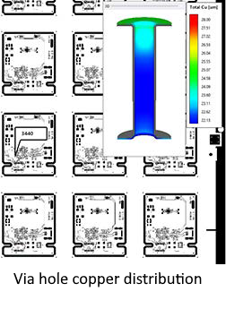
Simulation provides a graphical overview of the finished copper thickness distribution over the entire PCB panel. This overview enables CAM engineers to identify potential plating issues upfront and assess the most critical areas. As a result, they can inform the production team which PCBs need testing and which areas should these tests should focus on. They can identify particular vias and through-holes, where the presence of a sufficient copper thickness is a critical quality indicator.

Ultimately, CAE simulation lets CAM engineers deliver a better service to production. In particular, product testing can focus its resources on the most critical elements.

CAE simulation technology also allows process engineers to fine-tune copper plating production settings. 
fig 1
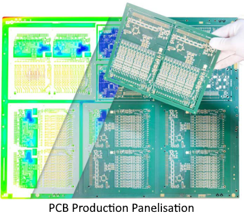
Using a digital twin of their in-house PCB plating tank, simulation enables process engineers to finish the work set in motion by PCB designers and CAM engineers. They can run in-depth what-if analyses and explore various scenarios for fine-tuning copper plating production settings. Possible what-if analyses include verifying the impact of layout modifications (such as the spacing in between individual panels), tooling (such as shielding, current robbers or auxiliary anodes), and process parameters (such as changes in imposed current density and total process time). And process engineers can do all of this without running any time-consuming trials in a real-world production environment.

Conclusions
CAE simulation software is a game-changing solution for production-proofing PCB copper plating. Notwithstanding the complexity of copper plating processes, this technology makes it straightforward to uniformize the finished copper thickness in the production of PCBs.
As improved copper thickness uniformity results in fewer out-of- spec products, production yield and profit margins significantly increase. With this technology this can be achieved without the need for any expensive prototyping.
The software can combine the specialities of PCB Design, CAM Engineering and Process Engineering to provide a game-changing solution for production-proofing PCB copper plating throughout all steps of the manufacturing process.  

fig 8

 Typical PCB Electroplating Line

  Elsyca, Belgium  Tel: +32 16 474960  This email address is being protected from spambots. You need JavaScript enabled to view it.  https://www.elsyca.com/plate/pcb-plating

 
  Go back to Contents


Section 7  ICT Christmas Seminar 2022: The Calibre of a ‘World Cup’ Event
 

bill wilkieRegardless of the potential distraction of the international football match between England and Wales in the World Cup competition, an enthusiastic crowd of PCB fans gathered in Meriden UK for the Institute of Circuit Technology Christmas Seminar, an eagerly-awaited networking opportunity that included a face-to-face industry welcome event and an outstanding technical programme.

1. New Insights into Selective Solder Nozzle Technology
The first presentation, delivered by Dr. Sam McMaster from the Functional Materials and Chemistry Research Group at Coventry University, was introduced by Technical Director Bill Wilkie, who began by remarking upon the success of Happy Holden’s recent series of engineering webinars. McMaster then shared his insights into wear mechanisms and future developments in selective soldering nozzles—a fascinating permutation of materials science, applied physics, and metal finishing in the practical context of a precision soldering technique that is currently growing in popularity.

sam mcmasterUsing video clips for illustration, McMaster described selective soldering as a process where individual through-hole components are soldered onto a PCB using a solder fountain programmed to move to each required position from underneath the assembly. The principal benefit of using a single-tube nozzle during this process is that each solder joint can be independently controlled with minimal thermal shock. This highly flexible non-contact process results in fewer solder defects.

Although current nozzle technology includes wetting and non-wetting versions for different applications, most of McMaster’s discussion concerned wetting nozzles. These have a limited-service life, and de-wetting issues during operation often cause increased maintenance downtime. The wear mechanism has been shown to be a complex mixture of corrosion and erosion effects. A KTP project is under way to develop a new base material with optimised composition, surface engineered for better wettability and increased lifetime, through corrosion resistance and initial wetting enhanced by electroplated and vapour-deposited coatings.

McMaster detailed the project methodology, from the evaluation of potential materials, coatings, and surface treatments, through to the production of initial prototype materials and new surface-engineered nozzles. New test methods have been established, mimicking real soldering conditions, to specifically study selective solder nozzles.

New insights have also been gained into the chemical reactions linking the wetting of solder to nozzles and the wear of nozzles. Alternative alloys and surface treatments have been developed to extend their lifetime and increasing their wettability; for commercial confidentiality reasons, however, McMaster refrained from disclosing further details during the presentation.

2. Flexible Circuits in Automotive Applications
Rapid growth in the utilisation of flexible circuits continues in automotive applications, especially in the electric vehicle (EV) sector. Representing a new corporate member of the Institute, Dr. Ioannis Kiratzis, chemical process engineer with Strip Tinning Flex, a division of Strip Tinning Automotive, introduced the company. Founded in 1957 and based in Birmingham UK, Strip Tinning has become a major supplier of components to a Tier 1 OEM base, specializing in antennas, smart glass, heating, lighting, and battery electronics.

ioannis kiratzisKiratzis discussed innovative solutions for EV battery modules, including flexible circuit applications for voltage and temperature control, and the manufacture of intelligent cell contacting systems for interconnection of individual cells within battery modules. He explained that, as a supplier to the automotive industry, the production part approval process is always a key consideration for the company. This industry standard outlines the process for demonstrating that engineering design and product specifications can be consistently met by the supplier's manufacturing process. Critical elements include accurate design records; a defined, monitored, and controlled process; and complete record-keeping and procedures for process failure mode effects analysis.

Strip Tinning Flex recently moved from screen printing to inkjet imaging. Their substrates include polyethylene naphthalate (PEN) and polyethylene terephthalate (PET) flexible polyester laminates, as well as polyimide; crimping is commonly used for solderless electrical connection in automotive assemblies. To meet growing demand, the company is currently focused on substantially expanding their flexible circuit manufacturing capacity.

3. Open Communication Produces High-quality Results
André Bodegom, managing director of Adeon Technologies in the Netherlands, now part of the CCI Eurolam Group, then delivered a powerful message in his presentation on industry cooperation: “Strong and open partnerships are a prerequisite for the real-time integration of design data and production results,” he said.

andre bodegom
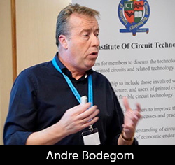
Bodegom began with some industry statistics and forecasts: The value of the global PCB market totaled $70.92 billion in 2020, of which the flex component doubled from 8% to 17% in recent years; the market is projected to reach a total of $86.17 billion in 2026 and as much as $130 billion by 2030. But although 93% of all production is currently coming from Asia, there is a clear trend toward increasing production in the U.S., followed by Europe. However, this shift will only happen if Europe makes a committed investment in greater automation in both hardware and software. Introducing and retaining intelligence throughout every stage of the manufacturing process is critical if Europe is to achieve better overall process control and alignment of different processes, with an aim toward higher traceability and self-learning algorithms.

Although increased growth is projected in European printed circuit board production after years of decline, the trend towards higher technology levels is the result of higher investment levels and growth in existing shops rather than an overall rise in the number of PCB factories in Europe. OEMs have inquired as to why they can’t get high-quality PCBs in the right volume in Europe anymore. The reality is that, over the last 30 years, OEMs abandoned their European suppliers by consistently buying from Asia. In the meantime, Europe has lost much of its capacity, and such capacity is not easily reinstated, especially at the technology and quality levels currently being demanded.

Bodegom has observed growing integration between design and the PCB, IC substrates, and EMS industries, with an increased demand for overlap between equipment, materials, and processes. He believes that the future lies in building strong teams and open partnerships with technical know-how to better support the entire electronics industry.

A fundamental element of future success is the sharing of data, and this, Bodegom said, must begin at the design stage. The vast majority of PCB design data is passed to the fabricator in Gerber format, which is an open ASCII vector format invented over 40 years ago that was intended to drive a photoplotter with basic machine commands. Using this format, all the intelligence built up during the design process is effectively lost at the output stage, forcing the PCB fabricator to try and recreate some of that intelligence at the CAM stage in order to create outputs for equipment like direct imagers, drill machines, AOI machines, electrical testers, etc., as well as chemical process lines. All this equipment not only uses data—it creates it. “What do we do with it?” Bodegom asked. “Practically nothing, other than occasionally using it retrospectively for tracing and identifying the cause of manufacturing defects.”

Adeon, together with some of its suppliers, has begun a project to gather that data, analyze it, and then feed it back into the loop—beginning with the design stage—to learn from the equipment how to control the manufacturing process. Bodegom re-emphasized that strong and open partnerships are a prerequisite for the real-time integration of design data and production results. Currently, much of the important data is not made available due to being blocked by machine suppliers for license reasons. Yet if that data could be read, it could be converted into a uniform communication link back into production. Artificial intelligence could then be used to analyze where improvements are needed. Bodegom gave several examples of equipment companies who are cooperating in the project.

4. Flexible Circuits Overcome Length Constraints
Back to flexible circuits—Philip Johnston, CEO of Trackwise Designs, introduced the intriguing concept of “Length-Agnostic FPC Manufacture.” The company, based in Tewkesbury UK, has developed a globally unique capability to produce multilayer flexible printed circuit boards of any length. In fact, they recently established a world record with an example circuit measuring 72 metres long. Johnston commented that the total length was governed only by the availability of suitable material.

philip jonston
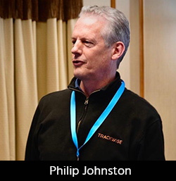
Trackwise’s key markets are in the automotive, aerospace, medical and scientific & industrial sectors. In automotive applications, flexible PCBs are suited to EVs in battery modules, battery packs, and battery management systems. Examples include 6-ounce copper weights, which can carry high-voltage power. In aerospace, large-scale flex (LSF) offers a 70% to 90% weight reduction in data cables and a 10% to 20% weight reduction in power cables. They can be used for fuselage-length or full-wing-width interconnects and are qualified for high temperature operation in harsh environments. At the other end of the scale, long, ultra-flexible, and finely-etched printed circuits have become key enablers for catheter-based distal electronics, with tracks and gaps as small as 50 microns.

Although Trackwise has started to adapt rigid-board manufacturing equipment, their proprietary technique is based on roll-to-roll processing and digital imaging. The company successfully transitioned from technology based upon repeated and separated images to a machine-intensive manufacturing processes capable of non-repeated and non-separated images. To do this, significant challenges had to be overcome in software development. Plating was achieved by adapting continuous plating lines built for volume manufacture; pressing, on the other hand, was achieved by adapting a continuous press built for the manufacture of copper-clad laminate. Ultimately, equipment suppliers who were prepared to “buy in” to Trackwise’s vision made this transition possible. Trackwise’s process is patent-protected worldwide. Their standard practice is to panelize all circuits, regardless of size, into a 100-metre production roll.

Whereas roll-to-roll flexible circuits are primarily used in passive interconnect applications, Trackwise also has the capability to carry out roll-to-roll assembly, which opens up the potential for active interconnect, “smart harnesses,” and flexible hybrid electronics.

Trackwise is extending their manufacturing capacity via a new factory, which is nearing completion and is fully equipped for length-agnostic roll-to-roll flexible circuit manufacture and flexible circuit assembly.

5. A Greener Future Through Recyclable PCB's
Recyclable PCBs was the topic of the final presentation by Steve Driver on behalf of Jiva Materials. He gave an update on the evolution of Jiva’s Soluboard material and its current positioning in the world of PCBs. “I also want to encourage you to think a little differently about how this technology may fit in our world in future,” he said.

steve driverDriver acknowledged that the Institute of Circuit Technology has always been an effective platform for launching new ideas. His challenge was how to change the mind-set: “Everybody always wants to talk about what things can’t do. I’m an optimist and try to make everything positive. This might not become commercially viable within our lifetime, but it could be just the start of something good!” He called on the industry to engage with the Jiva philosophy and to cultivate a “It might just work” mindset.

Discussing recycling issues in the context of a throwaway society, and the pollution created by end-of-life electronics where the typical recycling process involves shredding and incineration, Driver made it clear that people are looking for alternatives. The leading edge of the laminate industry currently appears more concerned with high-speed and high-power performance than with recyclability. But at the other end of the spectrum, innovators are looking for something new to get excited about.

So why Soluboard? Driver referred to the 57 million tons of waste electronic and electrical equipment produced every year and used the mobile phone, which is commonly replaced every two years, as an example. Although a phone can be recycled, chargers are generally thrown away. A charger contains a simple single-sided PCB that can be made on a Soluboard substrate. According to Driver, 1.3 billion chargers equate to 4.3 tons of PCB waste.

Producers of electronic goods are legally required to deal with waste. A case in point is TV set-top boxes, the disposal of which is an expensive responsibility; recyclable PCBs can be an economically attractive alternative. Jiva has continued to receive inquiries from interested companies and has successfully provided many solutions. Although Soluboard currently represents only a tiny segment of the laminate industry, its market share is growing steadily as Jiva continues its mission to tackle electronic waste with naturally-derived printed circuit board materials by reducing carbon emissions and waste electronic and electrical equipment levels.

6. Martin Cotton Awarded Honorary Fellowship
driver and cotton
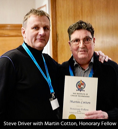
A very welcome seminar delegate was Martin Cotton, long-term supporter of the Institute and regular past presenter, who was determined to attend while continuing his slow recovery from serious illness. Everyone was delighted to see him and showed their sincere appreciation as he was awarded an Honorary Fellowship.

And the football score turned out to be 3-0 in England’s favour!


Section 8

Members News


Bill Miller - Prestwick Circuits Ltd.

bil miller service

Bill has already had an obituary placed in the Times Newspaper, but as a Fellow of the Institute, (Membership Number 556), it is fitting that we include our own thoughts in our Quarterly Journal. The Times obituary is available here.
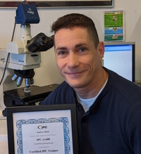
Bill came via Rolls Royce and Chris Rivett via STC in East Kilbride with a theme of producing circuits with good quality and a high standard of technology. Both came from an engineering background, Chris was a precision mechanical engineer and a skilled toolmaker and Bill added the entrepreneurship.

It is worth noting that they started from nothing, with premises in Prestwick (hence the name) and grew to having around 500 employees in the main plants in Scotland, which would have placed them in the top five in Europe at that time.

Bill was always pushing the technology element and made sure that they were first into HASL, ultrathin coppers, automatic loading vacuum presses and photo imageable solder masks like Probimer and Vacrel. They were also early adopters of Plasma desmear for multilayers and Digital Tooling via Scietex Technology.

With customer bases in Telecoms, Automotive and Computers, most large electronic companies were Prestwick customers, serving the USA, Europe, Scandinavia and the far East including Australia

The demise, which affected all of Europe, came with the low costs associated with the far East, with company size and scale of production pushing prices below what was achievable in the UK.

Bill was very well liked by all the Prestwick Circuits workforce and a highly respected figure in the PCB Industry worldwide. In the late seventy’s I attended a training event in Bournmouth and Bill came along on the last day and gave us a motivational talk. He was already an Industry giant and we were all grateful and impressed that he would take time out to address us newbies.

His achievements and common touch are writ large in the annals and history of the PCB Industry.

Bill Wilkie

With thanks and acknowledgment to Dr Peter Carmichael and Alison Miller

andy bunt

Andrew Bunt
Exception PCB

IPC CIT Certification

Andy Bunt is a now a Certified IPC-A-600 Trainer and will start an internal training programme for employees soon. We would like to congratulate Andy for his work achieving this certification.


Go back to Contents


Section 9

Industry News

Adeon Technologies BV

ACB Group invests in new Flying Probe System
ACB Group Invests in State of the Art Flying Probe Test System from ATG-LM:Atg 

atg probe

The ACB group is one of Europe’s largest independent manufacturers of highest technology printed circuit boards. The group consists of manufacturing facilities at Dendermonde (Belgium), Atlantec and Cibel (France) Read more...

Amphenol Invotech Environment and Sustainability
An interview with Hannah Whitmore Amphenol Invotec’s new Head of Environment and Sustainability Read more...
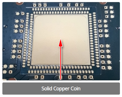
GSPK Circuits Innovative Copper Coin Thermal Solution

A copper coin is a solid piece of copper that is put onto or into the PCB, usually beneath the component or components that require cooling. When compared to a collection of thermal vias copper coins will produce roughly twice the cooling. copper coin

Additionally, the copper coin can offer direct contact between the heat-generating component pad and the heat sink in place of thermally conductive material. Compared to other conductive dielectric prepregs, copper has thermal conductivity that is typically 50–200 times better. Read more...

Minnitron Ltd.

Family Business Awards
We are proud to have been shortlisted for the 'Family Business Awards' Being in business for 60 years as a uk manufacturing company is unheard of and something we couldn't be more proud of. Wish us luck.
minnitron

Newbury Electronics Ltd Managing Director of Newbury Innovation
Conor La Grue, has been appointed to the position of Managing Director of Newbury Innovation, the design division of Newbury Electronics Ltd.
conor la grue
Newbury Innovation has grown significantly over the last 3 years and is now a major business unit within the Newbury Group. Read more...
Southern Manufacturing Southern Manufacturing & Electronics show will be held from
7-9 February 2023

The annual Southern Manufacturing & Electronics show is a firm favourite on
the calendar. Aerospace Manufacturing takes a closer look at what visitors can
expect to see at the Farnborough Exhibition Centre from 7-9 February 2023.
Taiyo

Taiyo Circuit Automation European Distributor for Shur-Loc Products

Taiyo Circuit Automation today announced a new partnership with Shur-Loc Fabric System. This partnership will combine Taiyo Circuit Automation world renown range of solder mask equipment with Shur-Loc’s unique screen making system. Read more...

Trackwise Designs plc Quality Assured at Trackwise Designs plc
Trackwise is delighted announce the successful completion of their AS9100/ISO9001 surveillance audit. The surveillance audit is a biannual process where the QMS processes are audited. This is to demonstrate “the ability to consistently provide products and services that meet the customer and regulatory requirements” Read more...
Ventec International Group

High Thermal Conductive Metal Base Laminate
Ventec announce the launch of its latest high thermal conductive metal base laminate VT-4BC designed for use in applications requiring excellent performance in thermal management including super bright lighting, power modules, controllers, motor drives and rectifiers. Read more...

  Go back to Contents


Section 10

Membership News 

bill wilkie
Bill Wilkie
Technical Director and Membership Secretary, Institute of Circuit Technology


New Corporate Members

Jiva Materials Ltd. Recyclable PCB Substrate
www.jivamaterials.com
Taiyo America Inc. Solder Mask and Printing Products
www.taiyo-america.com
 

New Member

Membership No Name Company
10555 Narisimha Murthy Virtulive Technology
 

New Associate Members

Membership No Name Company
10556 Dominik Matuszyk Ventec
10557 Ben Vaughan Teledyne
10558 Athula Kulatunga Purdue University
10559 Amba Prasad SMTA India
10561 Simon Fowler Graphic
10562 Neil Ford Graphic
10563 Ryan Tredgett  Graphic
10564 Phil Greenslade Graphic
10565 Ian Bond Graphic
10566 Matt Chant Graphic
10667 Phil Reed Graphic
10568 Mike Sargeant Graphic
10569 Ben Trenaman Graphic
10570 Simon Giddins Graphic
10571 Greg Hallatt Graphic
10572 Dom Henman Graphic
10573 Graham Farrington Graphic
10574 Louise Wood Graphic
10575 Dave Rich Graphic
10576 Sam Dyne Graphic
10577 Ian Brook Graphic
10578 Salvador Esposito Graphic
10579 Edward Stirland Graphic
10580 Garry Cross Graphic
10581 Chris Ford Graphic
10582 Rob Millar Graphic
10583 Henry Norton Graphic
10584 Paul Wells  Merlin PCB
10585 John Leafe Teledyne UK 
10586 Adam Whittall Teledyne UK
10587 Benjamin Watkin Loughborough U.
10588 Ellis Rankin Loughborough U.
10589 Joseph Fjelstad Verdant Electronics
10590 Dave Kemper Multicircuits
10591 Steve Laws XACTBCB
10592 Andrew Kelley XACTBCB
10593 Brian Sainsbury XACTBCB
10594 Joseph Quan Micro Arts Services
10595 Michael Theil Multicircuits
10596 Pradeep Menon Micropack India
 
  Go back to Contents    


Section 11 Corporate Members of the ICT  
Adeon Technologies BV adeon corp www.adeon.nl
Amphenol Invotec Ltd invotec corp amphenol-invotec.com
Atotech UK Ltd. atotech corp www.atotech.com
CCE Europe cce corp www.ccee.co.uk
CCI Eurolam cci eurolam corp  www.ccieurolam.com
Electra Polymers Ltd electra corp www.electrapolymers.com
The Eurotech Group  eurotech corp www.eurotech-group.co.uk
Exception PCB Solutions  exception corp www.exceptionpcb.com
Faraday Printed Circuits Ltd faraday corp www.faraday-circuits.co.uk
Graphic plc graphic corp www.graphic.plc.uk 
GSPK (TCL Group) gspk corp www.gspkcircuits.ltd.uk 
HMGCC hmgcc corp www.hmgcc.gov.uk
Holders Technology UK holders tech2 corp ww2.holderstechnology.com
Jiva Materials jiva www.jivamaterials.com
Merlin Circuit Technology Ltd merlin corp www.merlinpcbgroup.com
Merlin Flex Ltd merlin corp  www.merlinpcbgroup.com
Minnitron Ltd minitron corp www.minnitron.co.uk
Newbury Electronics Ltd newbury corp  www.newburyelectronics.co.uk
Photomechanical Services photomech corp  www.creekviewelectronics.co.uk
PMD pmd corp www.pmdchemicals
Stevenage Circuits Ltd stevenage corp www.stevenagecircuits.co.uk 
Strip Tinning Ltd strip tinning www.striptinning.com
Taiyo America, Inc taiyo  www.taiyo.com
Trackwise Designs Ltd trackwise corp  www.trackwise.co.uk
Ventec Europe ventec corp www.ventec-europe.com
Zot Engineering Ltd zot corp www.zot.co.uk 
     Go back to Contents


Section 12

ICT Council Members

Council Members

Emma Hudson (Chair), Andy Cobley (Past Chairman), Steve Payne (Hon Deputy Chairman), Chris Wall (Treasurer), William Wilkie (Technical Director, Hon Sec, Membership & Events), Richard Wood-Roe (Journal Editor & Web Site),  Jim Francey, Martin Goosey, Lynn Houghton, Lawson Lightfoot, Pete Starkey, Francesca Stern and Bob Willis, 

Go back to Contents


Section 13

Editors Notes

The ICT Journal

RickSue

Richard Wood-Roe
Journal Editor

Instructions / Hints for Contributors

1. As it is a digital format the length is not an issue. Short is better than none at all!

2. Article can be a paper or a text version of a seminar or company presentation. Please include data tables, graphs, or powerpoint slides. We can shrink them down to about quarter of a page. Obviously not just bullet points to speak from.

3. Photo's are welcome.

4. We would not need  source cross references

5. Title of presentation - Of course! Date, Job title of Author and Company represented.

6. An introductory summary of about 150 words would give the reader a flavour of what it's all about.

7. Style - we don't want out and out advertising but we do recognise that the author has a specialism in the product or process that will include some trade promotion. Sometimes it will be a unique process or equipment so trade specific must be allowed.

8. Date and any info relating to where or if this article may have been published before.

9. We can accept virtually any format. Word, Powerpoint, publisher, PDF or Open Office equivalents. 

10. Also, to make it easy, the author can provide a word file to go along with his original powerpoint presentation and I/we can merge it together and select the required images. 

11. A photo of author or collaborators.

I really do look forward to receiving articles for publication.

Richard Wood-Roe

This email address is being protected from spambots. You need JavaScript enabled to view it.

Go back to Contents