|
The Journal of |
| Section 1 | Editors Introduction |
|
Richard Wood-Roe |
In this issue of The Journal our first paper is an intriguing study of fine line etching of 16µm line pitch using software modelling to prepare the correct manufacturing parameters, with fabrication and assessment of the final product. Our second paper explores the additive manufacturing of pcb's using laser assisted deposition of conductive and dielectric layers. Our final paper identifies the importance of the phosphorous content of the nickel layer when measuring the nickel thickness of an ENIG coating. There is a review from Pete Starkey of the recent supplier webinars held in September. We have to report the passing of Harold Marshall, one of our industry characters. There is also the inclusion of industry and membership news. I hope you find the contents of the Journal interesting. I welcome your feedback. |
| Go back to Contents |

| Section 2 | Calendar of Events | |
Bill Wilkie |
2023 |
Details |
| September |
AUTUMN SEMINAR We replaced the Autumn Seminar in September with a series of weekly webinars to allow our Industry Supply Chain to showcase existing products. This is a departure for the Institute, since we normally focus on technical matters. Two slots of 30 minutes each, between 4 and 5pm each Wednesday. We had to reschedule the last webinar to suit Peplertech, with Andrew Norton being ‘on-passage’, Portugal to The Canaries, in a small yacht! Attendance: |
|
| December 5th |
Christmas Seminar Sponsored by local companies: Faraday Circuits, Fineline VAR and GSPK Circuits. |
|
| Go back to Contents | ||

| Section 3 |
Paper 1 |
|
Study on Wet Chemical Etching of Flexible Printed Circuit Board with 16‑μm Line Pitch |
|
|
Hui Li |
1.0 Abstract
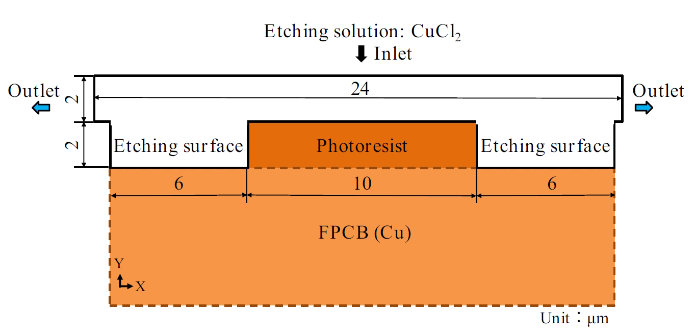
As high-precision flexible printed circuit boards (FPCBs) are required in electronic products, it is necessary to study wet chemical etching to obtain precise FPCBs with a 16-μm line pitch. First, a π-shaped FPCB model with 16-μm line pitch is established using the finite element method. The evolution of the Cu etching profile and the concentration and velocity distribution of the CuCl2 solution are then analyzed. To analyze the influence of conveyor speed and nozzle spray pressure on the Cu etching profile, wet chemical etching was tested along a horizontally conveyed line with CuCl2 as the acid etchant. The resulting profiles were analyzed by scanning electron microscopy. The experimental results agreed well with the simulation results, and the Cu etching profile obviously depended on both the conveyor speed and nozzle spray pressure. In addition, increasing the conveyor speed under constant nozzle spray pressure (0.16 MPa or 0.17 MPa) decreased the etching depth and increased the etching factor. In particular, when the conveyor speed was set to 3.8 m/min and the nozzle spray pressure raised to 0.18 MPa, the fabricated FPCB had a line pitch of 16 μm, an etching depth of 7.55 μm, and an etching factor of 6.45. This method can aid the selection of parameters for the wet chemical etching process, enabling the future manufacture of high-precision FPCBs and complex FPCB circuits. Keywords: FPCB · wet etching · finite element method · etching depth · etching factor 2.0 Introduction To lower the experimental cost, some researchers have numerically simulated the etching process. The common numerical methods included finite-difference time-domain simulations, the level set simulation method, and the finite element method. Time-domain simulations have revealed the influence of local surface curvature on the etch rate,24,25 3.0 Wet Chemical Etching Simulation 4.0 Reaction Principle and Simulation Method
Fig. 1 Two-dimensional geometric model of FPCB As the reaction proceeds, the Cu is dissolved and the CuCl2 solution is consumed. The etching reaction is:17 (1) Cu + CuCl2 → 2CuCl
where c denotes the CuCl2 concentration, D is the reactant diffusivity, and u is the fluid velocity.
To acquire accurate simulation results, the mesh division should be configured to a high mesh quality. Figure 2 shows the mesh quality of the etching cavity. The number of complete meshes was 7085 and the average and minimum unit masses were 0.85 and 0.17, respectively. 5.0 Simulation Results
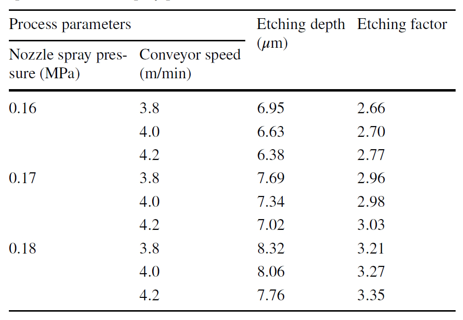
Fig. 3 Simulation results of etched profiles of FPCB under different conveyor speeds at nozzle spray pressure of Table I shows the simulated etching depths and etching factors at the three nozzle spray pressures and conveyor speeds. As the conveyor speed increased from 3.8 m/min to 4.2 m/min under a nozzle spray pressure of 0.16 MPa, the etching depth decreased from 6.95 μm to 6.38 μm and the etching factor increased from 2.66 to 2.77. At 0.17 MPa and 0.18 MPa, the corresponding decreases in etching depth were 7.69–7.02 μm and 8.32–7.76 μm, respectively, and the corresponding increases in etching factors were 2.96–3.03 and 3.21–3.35, respectively. In addition, both the conveyor speed and nozzle spray pressure clearly influenced the Cu etching profile. The etching depths at the above-specified nozzle spray pressures and conveyor speeds varied by a maximum of 1.94 μm. Table 1 Etching depth and etching factor under different conveyor speeds and nozzle spray pressures in the simulation.
As shown in Fig. 4a, the CuCl2 concentration at the inlet was 0.45 mol/L. The etching process starts from the Cu exposed on the etching surface and gradually proceeds toward the bottom. Both sides of the Cu are laterally etched by convection of the CuCl2 solution. The lowest concentration (0.38 mol/L) appears at the bottom of the etching cavity. At this location, the low concentration might be explained by insufficient replenishment of the CuCl2 solution after the reaction between CuCl2 and Cu; specifically, the spent CuCl2 solution cannot be replaced in time. As shown in Fig. 4b, the etching solution flows into the etching surface from the inlet and then flows from the outlets on both sides. The maximum and minimum veloci- ties are 2.25 m/s and 0 m/s at the outlets of both sides and the bottom of the etching cavity. The velocity distribution reveals an eddy current in the etching cavity caused by the convection circulation of the CuCl2 solution and the natural diffusion of CuCl2 on the etching surface. 6.0 Wet Chemical Etching Process 7.0 Fabrication of FPCB with 16‑μm Line Pitch
Fig. 5 (a) FPCB etching process and 8.0 Measurement of the FPCB Profile
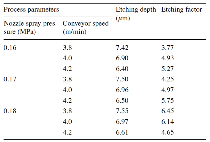
The FPCB profiles (see Fig. 7) were extracted along the etched surfaces in Fig. 6. Table II displays the experimentally obtained etching depths and etching factors under the three nozzle spray pressures and conveyor speeds. As the conveyor speed increased from 3.8 m/min to 4.2 m/min, the etching factor increased from 3.77 to 5.27 and from 4.25 to 5.75 at nozzle spray pressures of 0.16 MPa and 0.17 MPa, respectively. However, under a nozzle spray pressure of 0.18 MPa, the etching factor decreased from 6.45 at 3.8 m/min to 4.65 at 4.2 m/ min. It was considered that the complicated wet chemical etching process was influenced by more factors than the two-dimensional etching simulation. In general, enlarging the etching factor deepened the etching profile and increased the verticality of the sidewalls.
Fig. 7 Experimentally etched profiles of FPCB under different conveyor speeds at nozzle spray pressure of (a) 0.16 MPa, (b) 0.17 MPa, and (c) As additionally shown in Table 2, increasing the conveyor speed from 3.8 m/min to 4.2 m/min decreased the etching depth from 7.42 μm to 6.40 μm, from 7.50 μm to 6.50 μm, and from 7.55 μm to 6.61 μm at nozzle spray pressures of 0.16 MPa, 0.17 MPa, and 0.18 MPa, respectively. These etching depth trends are consistent with the simulation results in Fig. 3. In particular, at a conveyor speed of 3.8 m/min and a nozzle spray pressure of 0.18 MPa, an FPCB with of about 16-μm line pitch (the remaining Cu was 3.90 μm wide, the lateral etchings about the widths on both sides of the FPCB surface summed to 2.34 μm, and the bottom of the etching cavity was 9.45 μm wide in total) was successfully fabricated with an etching depth of 7.55 μm and an etching factor of 6.45. Table 2 Etching depth and etching factor under different conveyor speeds and nozzle spray pressures in the experiment
9.0 Conclusions Acknowledgments This work was supported by the National Key R&D Program of China Grant Number No. 2019YFB1704600 and the Hubei Provincial Natural Science Foundation of China Grant Number No. 2020CFA032. 10.0 References 1. S. Gupta, W.T. Navaraj, L. Lorenzelli, and R. Dahiya, Ultra-thin chips for high-performance flexible electronics. NPJ Flex. Electron. 2, 8 (2018). Published with approval from the author © The Minerals, Metals & Materials Society 2023 |
| Go back to Contents |

 (2)
(2) (3)
(3)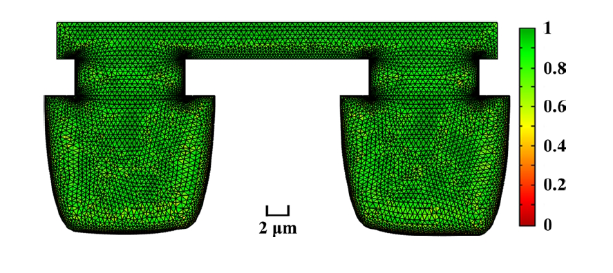 Fig. 2 Mesh quality of two etching cavities.
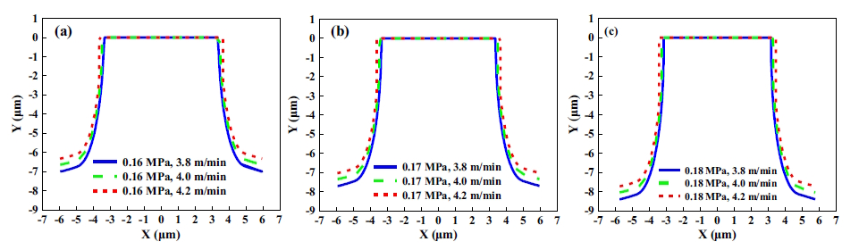
 To better understand the flow of etching solution in the etching cavity during etching, the concentrations and velocity distributions of the CuCl2 solution in the etching cavity have been analyzed at the intermediate conditions (nozzle spray pressure = 0.17 MPa; conveyor speed = 4.0 m/min), as shown in Fig. 4. The central blank region presents the remaining Cu. The concentrations and velocity distributions of the solution on both sides of the etching cavities are almost symmetric because the solution was sprayed evenly at the inlet. As shown in Fig. 4a, the CuCl2 concentration at the inlet was 0.45 mol/L. The etching process starts from the Cu exposed on the etching surface and the etching factor increased from 2.66 to 2.77. At 0.17 MPa and 0.18 MPa, the corresponding decreases in etching depth were 7.69–7.02 μm and 8.32–7.76 μm, respectively, and the corresponding increases in etching factors were 2.96–3.03 and 3.21–3.35, respectively. In addition, both the conveyor speed and nozzle spray pressure clearly influenced the Cu etching profile. The etching depths at the above-specified nozzle spray pressures and conveyor speeds varied by a maximum of 1.94 μm.
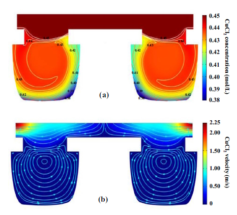 Fig. 4 (a) Concentration and (b) velocity distribution of CuCl2 solution in two etching cavities.
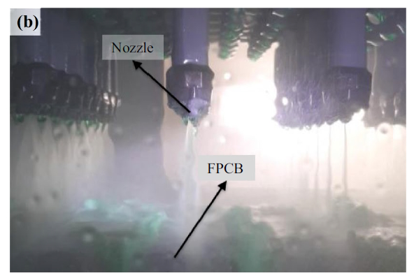
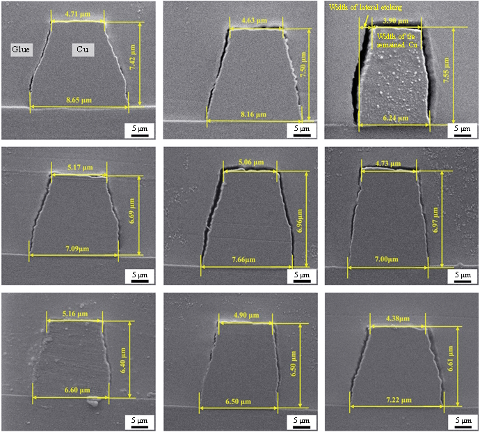 Fig. 6 SEM images of etched FPCB profiles under different conveyor speeds and nozzle spray pressures
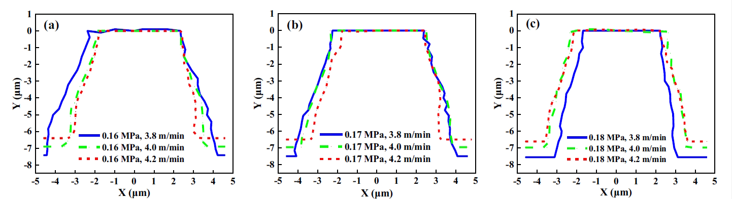
| Section 4 |
Digital and Environmental Circuit Board Manufacturing Based on Continuous Laser Assisted Deposition Michael Zenou, Ralph Birnbaum, Guy Nesher, Alex Stepinski |
||||||||||||
 Michael Zenou Michael ZenouChief Technonolgy Officer, ioTech Group Ltd. |
Abstract:
In the LIFT (Laser Induced Forward Transfer) technology, a material, evenly coated on a transparent carrier film, passes under a laser. The laser applies a short burst of energy to it. This releases perfectly consistent drops of material onto the substrate below. The material drops can then be sintered or cured inline, in the same machine. A great benefit is that this technology works for solder and polymers as well as for metals and ceramics. Multiple materials can be printed at the same time. This new technology opens the way to new advanced applications and the fabrication of innovative materials and novel applications. LIFT systems can work with many materials currently on the market and will also leave great freedom to innovate to both material engineers and chemists: they will be able to create products with significantly better properties than those achievable with current 3D printing technologies due to the low constraint requirement on the printed material. Viscosities can exceed 300,000 cPs and fillers of more than 40µm can be added. The current paper deals with one application of this technology, an innovative approach to manufacture circuit boards with the speed of printing. Keywords: new equipment, materials printing, laser assisted deposition, advanced manufacturing, additive manufacturing. 1. Introduction Additive Manufacturing has been around for roughly 3 decades. Even though it was the great hope for manufacturing, which today is roughly a trillion-dollar industry, additive manufacturing never really took a big share from the larger, manufacturing, industry. At roughly $21B, the additive manufacturing industry is just over 2% of all manufacturing and is used mainly as a prototyping tool. The reason for this is the material challenge. Today’s additive manufacturing technologies are generally not able to print the certified, industrial grade materials used in manufacturing. This is especially true in the electronics industry. They are generally too viscous for existing 3D printers. In their place, close approximations are usedi,ii, sometimes with more expensive, proprietary materials, that look like the real thing, but lack in mechanical and especially electrical properties and functionalitiesiii. Some applications where an additive manufacturing solution using original materials would be useful but don’t exist today, are for coating materials, epoxy filling and gaskets and conductive bonding materials. Ideally, the materials used for additive manufacturing would have to be the genuine certified industrial materials with all the desired characteristics in terms of temperature, viscosity, loading, etc. In electronics these would have to be printed at very high resolutions and accuracy. To make it economical, this would have to be done at high speed. And finally, since electronic components always consist of multiple materials, both organic and conductive, the solution must be able to handle multiple materials. 3D printing has made great progress in the past 3 decades, with huge advances in materials printing, but there is always some trade-off between these requirements. Laser Induced Forward Transfer (LIFT), a technology first developed in 1968iv and further developed ever since, can print materials with high viscosity, that hitherto, could not be printed. Materials with viscosities higher than 300,000 cPs can be printed. The technology has successfully been tested on silicone, ceramics, conductive epoxies, and metalsv. The resolution of the system currently goes down to 30um. In the same print, varying resolutions from 30um to 500um can be printed. Depending on the implementation, multiple different materials can be printed simultaneously, including polymers, metals and ceramics. This is all done at high speed, reaching 3 liters/hour, or 2,000 drops/second. All along the electronics supply chain, there are areas where one material is being deposited, printed, etched… onto another. This is true for PCB, SMT assembly, semiconductor packaging, as well as for EMS. 2. The Technology
Fig 1: Continuous Laser Assisted Deposition The technology is contact-less, and does not make any use of masks, stencils or cloggable nozzles. Materials with very high viscosity, over 300,000 cPs can be printed. All post-processing is inline. Both UV and thermal curing is completed in the same station, thereby saving both time and space. Laser sintering and ablation are also performed Compared to existing technologies, such as screen printing, or jet dispensers, LIFT offers great benefits. Traditional digital technologies are defined by the nozzle size, which limits viscosity, speed and resolution. Traditional non-digital technologies are defined by the mesh size, which limits the layer thickness and resolution. Laser Induced Forward Transfer technology has neither nozzle, nor mesh, giving it full flexibility. It has all the digital flexibility of jet dispensers, with the ability to print multiple materials on multiple layers. With throughputs comparable (but not quite equal to) screen printers. Resolutions are greater than either jet dispensers or screen printers. No nozzles to clean, and no stencils to maintain, reduces the maintenance costs of LIFT technology To summarize: 3. Applications
Figure 2: single layer PCB showing both copper metallization Different type of coating can be printed like solder mask, waterproof, glob top, and others. Adhesives of all types can be printed, such as solder paste, conductive epoxy, two component epoxies, and others.
Fig 3: Complex conductive layer geometry from Gerber file. There are additional applications in the SMT world. Solder paste is a prime candidate for this technology, and several different standard solder pastes have been successfully printed. Resolutions of solder paste balls go down to 100µm solder ball diameter for Type 6 solder paste. Being a digital technology, both large and small components can be printed in the same print, even printing on other components, for multiple chip stacks. As a comparison, some of the fastest jet dispensers reach on the order of 100,000 solder balls/hour. This technology can go over 7,000,000 solder balls/hour. Die bonding is an application that has been shown to have benefits with this approach too. A variety of adhesive pastes have been tested, with high flatness uniformity. Throughputs can be higher than 10,000 droplets/sec. A wide range of other adhesives can be printed with resolutions down to 50um, including unusual shapes with sharp corners and curved sides are not a challenge. Throughputs over 300mm/sec and high accuracy, below 5um. Multiple adhesives can be printed together LIFT offers a fabless solution to inner-layer PCB manufacturing. The new process will print inner layers digitally, substantially speeding up inner layer process, for multi-layer boards and HDI layers. The process delivers metallization and dielectrics in an additive manufacturing way. Multiple layers can be printed, printing the filled vias as the process builds up. The outer layers are then finished with traditional processes. If desired, the solder mask, pad finish and legend using industrial grade materials can also be printed with the same LIFT process.
Fig 4: 3-D representation of features. 4. The Multilayer Process The new hybrid process involves building up the inner layers, one layer at a time. The dielectric layers are laid down together with the via interconnects, followed by the conductive circuity on top. The feature sizes the LIFT process can currently support are shown in Table 1.
Table 1: Feature sizes for hybrid PCB process using C.L.A.D A copper trace can be deposited with a width of 50µm. The system laser can then be used to ablate the copper, trimming it down to 30µm. Vias size down to 60 µm can be filled with copper.
Print timings of a PCB layer are shown in Figure 5. Printing the metal traces, dielectric layer, and via interconnects, can be done in roughly 15 minutes. No drilling is required, since the via interconnect is printed on the fly, together with the dielectric layer. More via interconnects won’t increase the timing. There is no additional cost to complexity with additive manufacturing. The hybrid approach to printing a multi-layer HDI board with LIFT technology starts with a plain copper sheet that is used by the industry today, the copper sheet could be a plain sheet or a metal coated sheet. For example, copper coated with a thin film of copper on top or other metal in any thickness. A dielectric layer and the metal layer are deposited on top of the copper sheet in very high resolution one layer after the other. The LIFT technology allows any number of materials, so both dielectric and copper can be printed at the same time in any sequence that will support the final properties. It is also possible to add post-processing during the printing sessions when needed and ablate excess of material or sinter the metal traces where necessary. The same laser for the LIFT process can be used for laser ablation, and for sintering the copper. A UV lamp can be added for the dielectric polymerization as well as a thermal source for drying. If a copper trace is required smaller than the deposition limits, it can be ablated down to 30µm, leaving no residue on the dielectric. The manufacturing of the next layer will be identical, only instead of copper traces, the via interconnects are printed simultaneously with the dielectric. The microvias are built up as the layers are built up, so there is no drilling involved. This process is repeated for as many layers as required: After the final inner layer is laid down, an additional copper film is used as a top layer. This is then placed in a thermal press to shrink and bind. The two outer copper layers can then be removed, leaving a sandwich of two thin copper films, with multiple HDI layers in between. To summarize: This process combines the benefits of the LIFT technology without the need to recertify the inner layers with the final customer. 5. Summary and benefits The benefits of the LIFT technology are: • The technology supports multi-material deposition: Conductors, dielectrics and solder mask This technology can give a substantial boost to a high-mix, low-volume shop. There are no overhead costs, such as would be with screen printing technologies, and as there is no cost to complexity, designs that are currently produced in weeks, can be done in an hour. Since the outer layers are not touched, the customer usually doesn’t interfere with the production process. This will speed up the manufacturing process, while reducing costs. The technology could prove to be a big boost to on-shoring PCB production in the near future. i M. Zarek, M. Layani, I. Cooperstein, E. Sachyani, D. Cohn, S. Magdassi, Adv. Mater. 2016, 28, 4449. |
||||||||||||
| Go back to Contents |
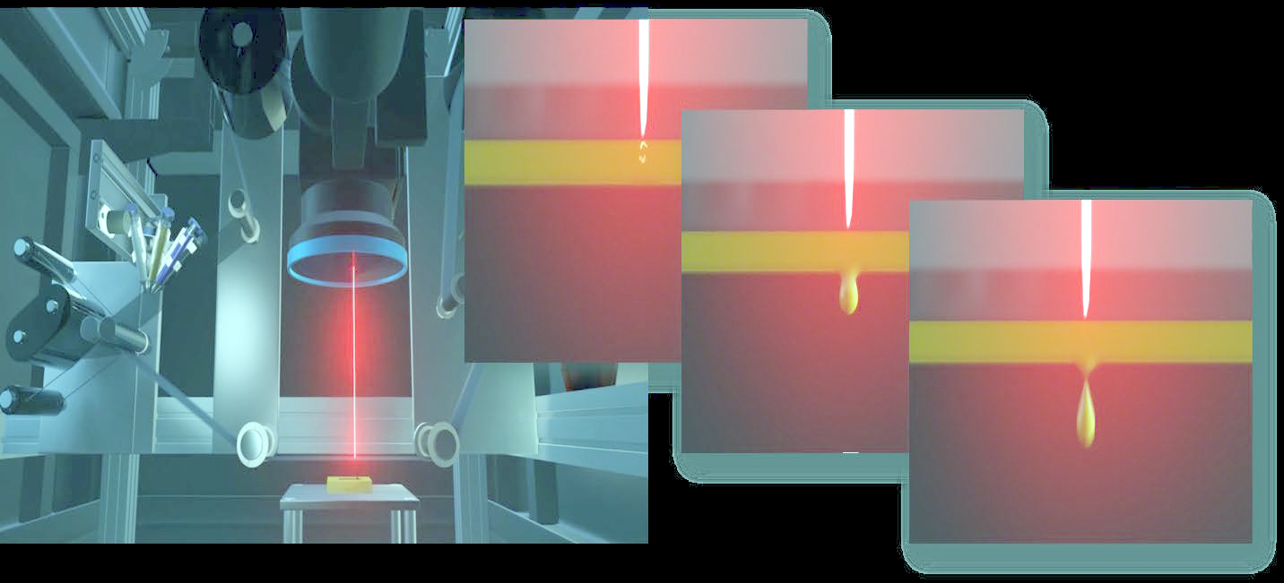
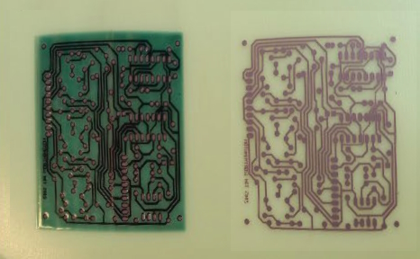
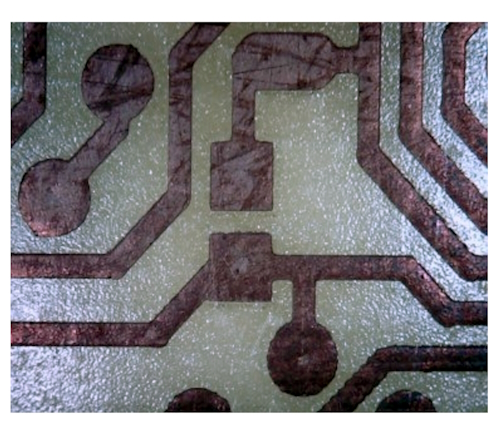
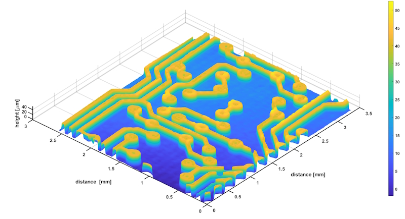
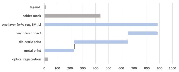 Figure 5: Print timings of 250mmX250mm PCB layers
| Section 5 |
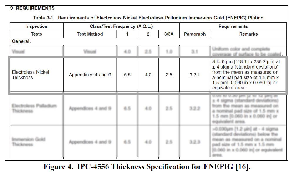
Understanding Electroless Nickel Thickness in ENIG and ENEPIG |
|
Robert Weber |
Abstract Introduction The background for thickness range requirements for electroless nickel arise from both practical and physical requirements. IPC-4552B indicates electroless nickel thicknesses below 3 μm may be appropriate for high frequency applications[6]. However, electroless nickel thicknesses below 1.27 μm [50 μin] are not recommended due to increased potential for copper diffusion through the electroless nickel layer[7]. Practically, the time to deposit 1.27 μm of electroless nickel is shorter than the time to deposit the required thicknesses of immersion gold, especially important on an automated plating line. Plating the minimum 1.27 μm would require freshly deposited nickel PWBs to be placed into a “holding station” or rinse water tank for an extended period. This risks passivation of the nickel prior to the immersion gold (or palladium) deposit. Passivated nickel presents problems with the adhesion and solderability of subsequent plating layers. To minimize hold times and potential impact on the nickel, the minimum thickness established at 3 μm. This was found to work well with automated plating lines, as well as providing an excellent minimum thickness for wire bonding. The maximum thickness of 6 μm [236.2 μin] was incorporated to prevent high insertion forces and, therefore, possible damage for press fit pins into PWB through holes[8]. X-ray fluorescence (XRF) instrumentation is the only accepted IPC-4552B metrology method[9] to measure thicknesses for plated layers. IPC-4556 does not restrict ENEPIG thickness measurements to XRF but Appendices 4 and 9 highlight and detail specific guidance and considerations for use of XRF to measure ENEPIG[10]. XRF instruments calculate thicknesses by determining the amount of mass of material present in a defined measurement area. The analysis, or measurement, area of a specific XRF measurement is colloquially known as the “spot size.” The spot size is defined by type of XRF system used, either with mechanical collimators or polycapillary optics. IPC-4552B specifies the use of either a 0.3 mm or 0.6 mm mechanical collimator, or using a system equipped with polycapillary optics (measurements made with polycapillary optics shall be made with a scan over the surface)[11]. IPC-4556 does not directly specify a spot size, but does state that measurement spot size “shall not exceed 30% of the Calculation of coating thickness using XRF, while complicated, can be simplified to a core principle: measuring the amount of mass of material within a known measurement surface area. The measurement surface area is defined by either the collimator size or polycapillary optic spot size. An XRF instrument observes and quantifies an amount of mass of material, uses known or user input for the density of the material, and calculates a thickness value. Thus, calculating the thickness of electroless nickel thicknesses presents challenges. Electroless nickel is a self-sustaining, autocatalytic reduction process using hypophosphite chemistry[13]. As the nickel deposits on a substrate, by design, a quantity of phosphorus is incorporated within the nickel layer. The addition of phosphorus changes the density of the deposit. As described in the paragraph above, XRF measurements use mass in a defined surface area to derive a layer thickness. Changes in density, if not included in the measurement calculation, will present themselves as a change in layer thickness. Accurate measurement of the electroless nickel layer thickness is possible if a user corrects for density changes caused by the inclusion of phosphorus in the nickel deposit in a specific sample. The thickness measurement can be calculated with the appropriate density (e.g., fixed percentage; 92% Ni, 8% P) of the specific sample. Some XRF instruments are capable of directly measuring the phosphorus content (calculating the alloy percentage in wt.%) in each sample and will automatically calculate a thickness with the correct density. Experiment
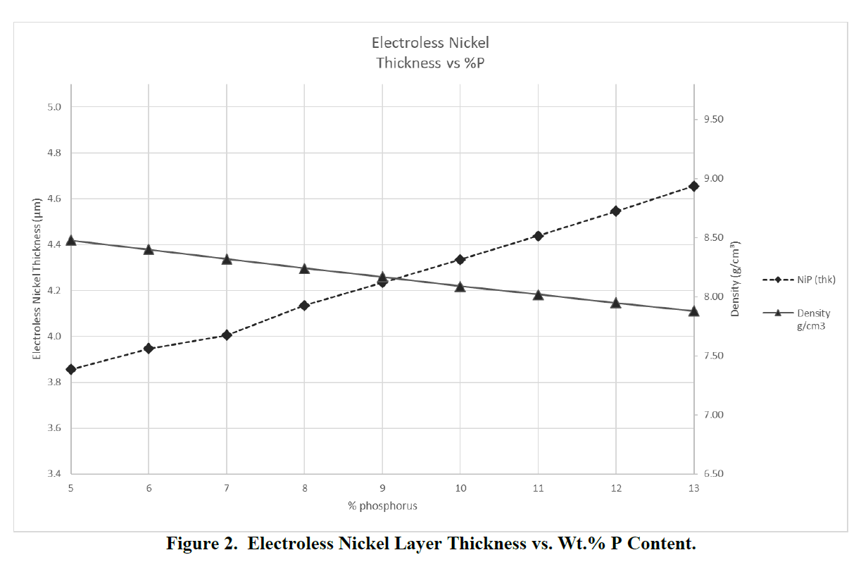
The sample was measured five (5) times under repeatability conditions[14] (same person, same location, short time frame, same instrument, etc.). The phosphorus content was initially set at 5%; the measurement calculation recipe was then manually adjusted (Figure 1) between each group of measurements, in increments of 1%, to a final value of 13 wt.% P. Mean values and standard deviations were calculated from the individual measurements (Table 3). The calculated thickness was plotted vs. the wt.% P used in the measurement calculation (Figure 2).
Discussion
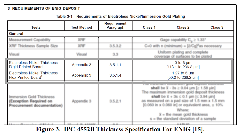
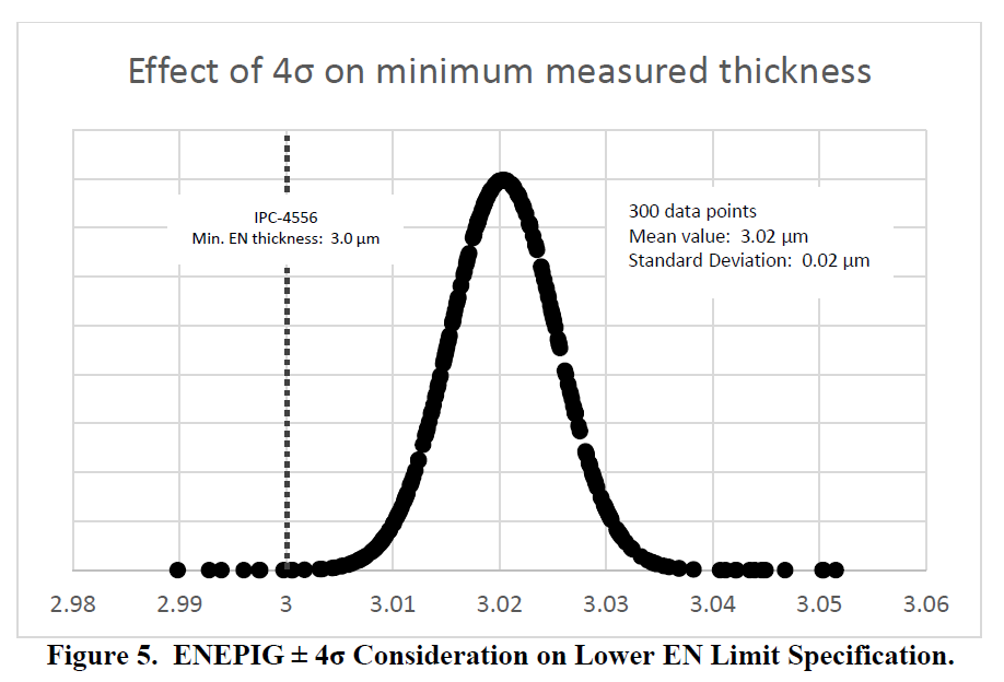
The risk of rejecting good parts, or conversely accepting failing parts, is real if we accept or reject solely on the thickness of the electroless nickel layer. Recall from Figure 2 and Table 3, the dimensional thickness of the electroless nickel layer is affected by phosphorus content in the layer. From Table 4, we see how an understanding of these effects is critical when the sample is at, or near, the specification’s tolerance (Figure 3, Figure 4). Referring to Table 4, the sample, as measured at 8% phosphorus, will pass both IPC-4552B and IPC-4556 minimum electroless nickel thickness but will fail if the sample is measured at 7% phosphorus. The potential for false rejection or acceptance increases when we look at ENEPIG and IPC-4556. As mentioned earlier from Figure 4, with ENEPIG, the standard deviation of the electroless nickel measurements must also be considered. Figure 5 shows a plot of 300 randomly generated data points. In this case, using the measurement standard deviation (1σ) of 0.005 μm from Table 4, the part must measure a minimum of 3.02 μm to meet a minimum thickness of 3 μm ± 4σ.
Conclusion Both IPC specifications apply a 3–6 μm [118.1–236.2 μin] thickness specification to the electroless nickel layer. This creates potential problems for both the PWB manufacturer and the end user; there may be false rejections or acceptance because an incorrect phosphorus content was used to calculate the thickness. This potential thickness measurement error is most relevant for parts with electroless nickel thickness at, or very close to, the minimum or maximum tolerances. Care should be taken to use the correct phosphorus content for the sample being measured or use XRF instrumentation capable of directly evaluating the wt.% P in the sample being measured. References |
| Go back to Contents |

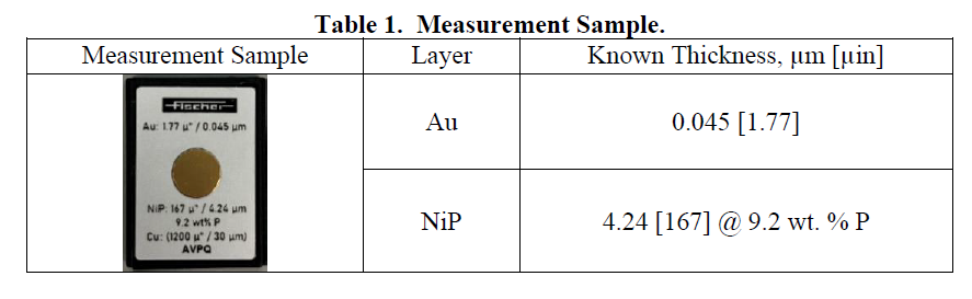
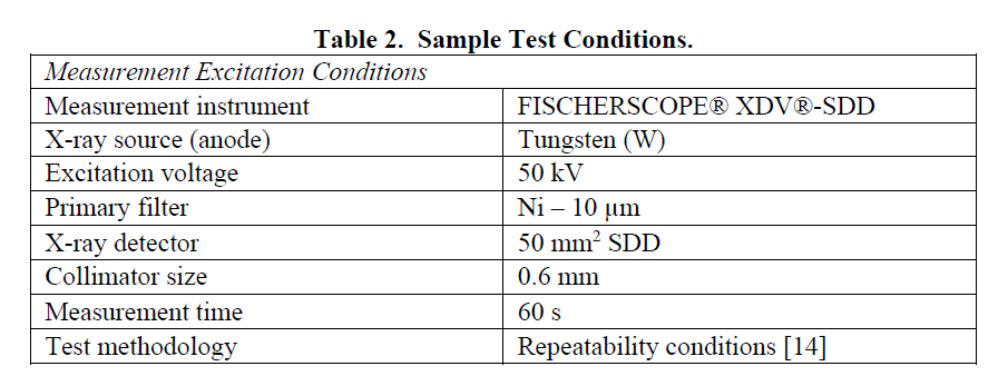
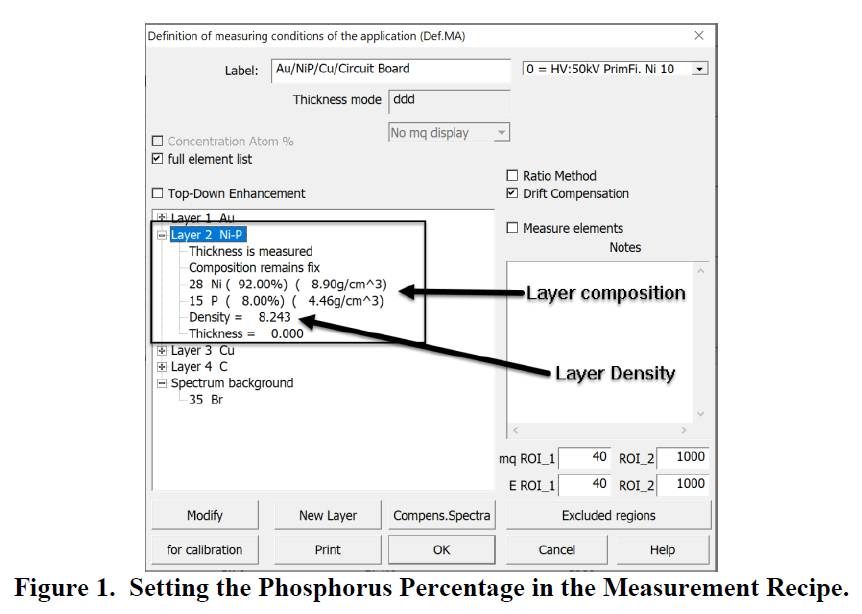 Fig 1: Setting the Phosphorous Percentage in the Measurement Recipe
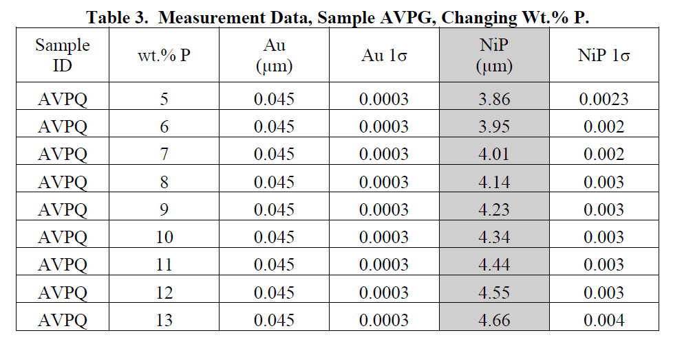
 Additional testing was performed on a second sample to evaluate how different percentages of phosphorus affected electroless nickel thickness measurements near the lower limit of the IPC specifications. Testing was performed using a certified electroless nickel sample at 3.05 μm [120.1 μin] containing 8% phosphorus over a solid copper base. The phosphorus content for the thickness calculation was manually varied, in the measurement settings (Figure 1), from 5 – 10 wt.% P. This data is displayed in Table 4.
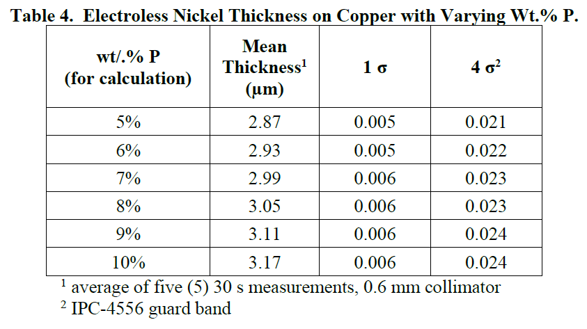
| Section 6 | Suppliers September Wednesday Webinars. |
|
1.0 Introduction |
|
|
Neil Chamberlain |
2.0 Polar Instruments The series began on September 6th with Neil Chamberlain, Polar Instruments European Sales Manager, emphasising the importance of making the right decisions at the right time in the design process. Long recognised as a leading expert on signal integrity, and always happy to share his encyclopaedic knowledge of PCB stackup tools, modelling, testing, and documentation for impedance control and insertion loss, Chamberlain took the viewpoint of the PCB fabricator, a significant part of whose task was to predict the effects of his manufacturing process on the materials selected and the geometries chosen by the customer. Some of the decisions taken after the customer’s data had been received would affect the impedance. But so would some decisions already made, consequences of the limitations of the design and outside the control of the fabricator. Provided that there existed a good working relationship between fabricator and customer, there was an opportunity to use modelling tools and to discuss design parameters very early in the design phase. Some of the customer’s primary decisions were made well before commencing the layout: decisions about what would be the stack-up and what would be the trace geometries. Those decisions influenced what materials would be selected and how the board would be manufactured. Some of Polar’s tools for design and documentation of the stack-up could be used to help the customer make the right decisions at the right time in the design process. But when the fabricator had no prior involvement until the data arrived at the factory, and needed to carry out an analysis and maybe make dimensional adjustments in CAM before proceeding to manufacture, Polar had tools available to calculate the effect on impedance of those changes. The Si8000 was a quick-solver interface, which Chamberlain equated to a pocket calculator, simple and intuitive to use, but with some limitations. A more elaborate tool was Speedstack, which used parameters from a comprehensive materials library and not only predicted how the complete job would work in terms of impedance, but could output gerber data for a meaningful test coupon to be incorporated on the manufactured panel. Then, at the end of the manufacturing process, Polar’s test equipment could be used to verify that what had been calculated had actually been achieved, and to produce a report that could be sent to the customer. Chamberlain gave many application examples of the Si8000 tool, which offered a choice of about 120 different structures that might be required by the customer. He demonstrated a consequence of “getting it wrong” using two structures that appeared similar but where cores and prepregs were transposed with respect to impedance structures within the stack. One structure gave a calculated 70 ohms, the other gave 53 ohms. He explained how the Speedstack tool gave the operator the opportunity to decide what material would be used and how the stack was to be put together – effectively defining the rules of the stack so that the system could use this information and make the allocation of the impedance structures a straightforward procedure. Speedstack featured an on-line material library, Polar having established working relationships with most material manufacturers world-wide and listed all of their relevant material parameters in a consistent format. Therefore fabricators could use specific products from their preferred suppliers in the knowledge that all of those parameters were readily available and could be used directly by Speedstack. The tool analysed how the materials would behave in-process, including press thicknesses and effective local resin contents depending on the copper pattern characteristics of individual layers and how the stack had been put together. The completed stackup was presented in a report that could be exported in a choice of formats and, if required, used to advise the customer how it was intended to build the board. |
|
|
3.0 Ventec International Group What laminate to use? Leigh Allinson, Technical Sales Director at Ventec International Group, gave an update on Ventec’s extensive materials range, discussing properties and applications. He began with a brief review of the company’s history and growth, from the original Suzhou plant in 2000, the foundation of Ventec Europe in 2006, Ventec USA in 2007 and listing on Taiwan Stock Exchange in 2019, to its current position as a world leader in the production of high performance copper clad laminates and prepregs, with four manufacturing facilities in Asia and seven fully-equipped service centres across the globe, managed by a team of industry specialists from China, Taiwan, USA and Europe, with a focus on quality, technology, customer service and effective supply-chain management. Their whole supply chain was fully accredited to the aerospace quality standard AS9100. Allinson summarised Ventec’s product range which, besides standard FR4 and polyimide laminates and prepregs included materials for thermal management, signal integrity, RF/microwave and IC packaging, as well as for lead-free assembly. There was also a full range of Ventec halogen-free laminates and flex and flex-rigid materials. Ventec acted as distributors for thermal interface materials, lamination consumables, drill entry and exit materials, copper foils and Taiyo solder mask products. Allinson gave details of the tec-speed family of RF and high-speed digital materials, including PTFE ceramic, PTFE random glass fibre, and hydrocarbon ceramic with and without woven glass. He described Ventec’s polyimide range and showed the roadmap for tec-thermal thermal management laminates and prepregs. He continued his description of Ventec’s product families with the tec-pack series of IC package substrates, special applications materials, low-flow and no-flow prepregs and illustrated the properties of Ventec high-voltage anti-CAF laminates. To complement Ventec’s extensive range of materials, the group now incorporated Giga Solutions, a leading distributor of PCB manufacturing equipment, headed by Ramesh Dhokia who brought 25 years of experience in providing turnkey solutions. |
|
|
4.0 Isola Group The second in the Wednesday Webinar series, on September 13th, featured presentations on speciality laminates and engineering solutions. There is an increasing demand for non-PTFE and non-thermoplastic based substrates with dielectric properties similar to PTFE, with high glass transition temperatures and high thermal reliability, together with stable dielectric properties over a higher range of temperatures and frequencies. Jim Francey, RF Business Director Europe with Isola Group, described two low-loss materials from Isola’s extensive product portfolio: Astra MT77 for RF/microwave and I-Tera MT40 for high-speed digital designs. He explained that a remarkable characteristic of Astra MT77 was its ultra-low dissipation factor of 0.0017, which made it a cost-effective alternative to PTFE, especially in millimetre-wave radar for automotive applications, while offering straightforward PCB processing compatible with normal FR4 procedures, without the necessity for plasma treatment. It was not ceramic-loaded and therefore did not cause excessive drill wear. The material was based on a thermoset resin system and could be laminated using standard press cycles and mixed with FR4 and other materials in hybrid builds, being capable of multiple lamination cycles where necessary. Finished multilayers were CAF resistant and compatible with lead-free assembly. Francey illustrated the comprehensive range of cores and prepregs available, listing resin contents and glass styles, and using actual test results to demonstrate the consistency of dielectric constant and dissipation factor over frequencies from 2GHz to 20GHz, temperatures between -40°C and +140°C, and after long-term ageing at 125°C. The thermoset resin matrix exhibited very good adhesion to metals, enabling the use of copper with extremely smooth surfaces. He demonstrated the benefits of using HVLP foil which minimised loss and, in combination with accurate thickness control in the manufacture of core laminates, contributed to the uniformity of dielectric constant. Using the example of an 8-layer any-layer plated via construction for a cognitive-antenna radio system he commented that the thickness uniformity ensured that planarization could be carried out consistently and reliably. Concluding that Astra MT77 ultra-low-loss laminates and prepregs represented a breakthrough product for millimetre wave frequencies and beyond, Francey turned to his second featured material: I-Tera MT40, a next-generation family of very-low-loss laminates and prepregs, again exhibiting exceptional electrical properties, very stable over a broad frequency and temperature range, and particularly suitable for high-speed digital applications as well as RF/microwave designs. With its very low dissipation factor of 0.0028 – 0.0035, I-Tera MT40 offered a cost-effective alternative to PTFE with the added benefit of processing like FR4 and not requiring the special through-hole treatments associated with processing PTFE-based laminates. It also exhibited remarkably good thermal stability, as demonstrated by passing 1000 cycles of HATS testing with no failures. |
 Gavin Barclay Gavin BarclayACS Industries |
5.0 ACS Industries “Forty-two years in the business of holes” was how Gavin Barclay, Commercial Director of ACS Industries, introduced his company which has been supplying carbide tools and providing contract drilling and routing services to UK printed circuit fabricators since 1981. He explained the company’s three main areas of operation: subcontract drilling, carbide tool supply and drill re-pointing. The drilling operation involved rather more than pressing the “cycle start” button, and Barclay explained the engineering procedure step-by-step from initial data input to final inspection. The term “subcontract drilling” represented much more than simply overload-capacity – there were many situations where customers had taken-on jobs that turned out to be more difficult than they had initially believed, whether in size or technology, and had turned to ACS as the experts in resolving their problems. ACS had full x-ray capability for inspection and measurement of drill registration on multilayers, and were prepared to work closely with individual customers to make scaling adjustments where permissible. The second part of ACS’s business was the supply of carbide cutting tools, with the largest stock of PCB tools in the UK and representing Union Tool, HAM and Performance Micro Tool, which gave ACS a very comprehensive range and the advantage of being able to supply off-the-shelf for next-day delivery, or consignment stock where required. Barclay described the different types of tool available, from micro-tools as fine as 0.05mm to 0.25mm, standard drills; undercut drills up to 1.6mm. He explained the differences between single-flute and parallel-flute drills, the latter becoming the more popular in the industry. Special slotting drills were more rigidly constructed for nibbling slots at the time of drilling, rather than as a separate routing operation. There were different types of router: diamond-cut and chip-breaker being most common, the former being more hard-wearing and the latter giving a finer surface finish. And there were several other formats available for special purposes. And the third main part of the business was drill re-pointing. Barclay described ACS’s equipment and inspection facilities, and showed lots of horror-story examples. But ACS obviously preferred to work with customers who supplied drills with controlled even wear that could be successfully re-pointed several times. He did remark that special-purpose laminates loaded with abrasive ceramic fillers contributed to rapid drill wear, and stressed the importance of establishing meaningful drilling machine parameters – different materials required different feeds, speeds and hit-counts. ACS had many years of experience running their own machines on which to base their in-house tool management procedures. ACS firmly believed that by working with them, either as a tool and re-point supplier or as a subcontract service provider, the fabricator could improve drill-shop productivity, hole-wall quality and positional accuracy, and make overall cost savings. |
|
Andre Bodegom |
6.0 Adeon Technologies The third in the Wednesday Webinar series, on September 20th, featured presentations from Adeon Technologies, specialist in the service and distribution of capital equipment for the European printed circuit board manufacturing market, and its parent group CCI Eurolam, multinational supplier of PCB laminates and process materials. Adeon’s MD, Andre Bodegom, began with the company’s mission statement which accentuated the philosophy of partnership with the European electronics industry, to enable its customers to meet their critical business objectives by providing solutions for the fabrication and assembly of professional electronics through hardware and software systems and services, all fully supported by its own service engineers. He added that Adeon constantly monitored and improved its own performance and had successfully built a track record of being a reliable and innovative partner to its customers. Based in the Netherlands, Adeon had been a professional supplier to the UK PCB market since 1992, with an emphasis on service performance, operator training and tailor-made predictive maintenance. Adeon had established sales and service partnerships with a long list of carefully selected suppliers. These included atg-LM electrical test systems, Boffotto plasma treatment systems, CIMS AOI systems, DIS Technology optical registration and bonding systems, Dynachem lamination and spray coating systems, LHS inkjet legend printing systems, Mach3La: x-ray registration drilling and x-ray inspection systems, Mass via filling and planarising systems, WISE wet process lines, Süss MicroTec inkjet soldermask systems, Ucamco CAM software solutions, photoplotters and direct imaging systems, and VF drill-stack preparation equipment, each with its dedicated engineering team. Adeon were also European sales partner for XACT-PCB process registration control, and service and sales partner for Benmayor automation solutions linked to the Adeon portfolio. |
|
Mark Gordon |
7.0 CCI Eurolam group Based in France, CCI Eurolam have been supplying the electronics manufacturing industry for 55 years, the original company having been founded over 100 years ago and still family-owned. The group had expertise in a wide array of electronics manufacturing technologies, covering the PCB fabrication and assembly industries, through ceramic circuits and printed electronics to semiconductors. It was active through a complex electronics ecosystem in the EMEA area, with business units in Germany, UK, Spain and Netherlands. Mark Gordon, Managing Director of the UK operation, explained that the group had 150 employees, including 35 sales engineers and 17 applications engineers, and the ability to communicate in 14 spoken languages. |
|
This was a very successful format and went down well with the attendees and presenters: |
|
| Go back to Contents |
 Leigh Allinson
 Jim Francey
 We are sorry to have to announce the passing of Industry stalwart Harold Marshall. Born in Bolton, Harold attended Sunning Hill primary school and Bolton County Grammar, founding Vantage Circuit Products Ltd in 1987. Harold was an electro-chemist and worked initially in the laboratory at the former De Havilland aircraft works in Lostock and held senior positions in Imasa Silvercrown before branching out on his own with Chemlec Solutions and latterly with Vantage Circuit Products in Farnworth. He also spent time at TDS during their hay day in the 1980’s. Harold was a very gregarious individual, who always attended the many industry events and was sure to be found on his feet asking questions and thanking speakers. He was a very determined character, who threw himself into every venture, always ready to prove a point or have a jest. He was good company, enjoying his London club and the frequent outings as the pcb Industry expanded.
|
Industry News |
|
| Exception PCB | 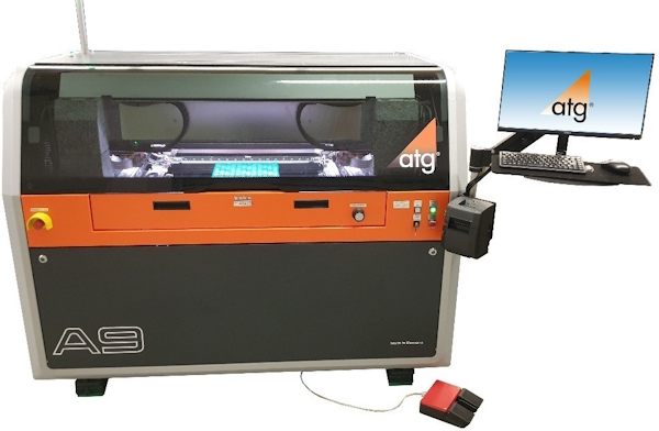 Exception PCB are excited to announce it has installed 2 new A9 flying probe test systems from atg-LM, the market leaders in electrical testing of Printed Circuit Boards to perform electrical tests more quickly and efficiently. The atg-LM A9 technology brings unrivalled test speed and accuracy with the latest linear drive technology and it performs at a rate of up to 220 measurements per second! The new flying probe test… Read More » Exception PCB are excited to announce it has installed 2 new A9 flying probe test systems from atg-LM, the market leaders in electrical testing of Printed Circuit Boards to perform electrical tests more quickly and efficiently. The atg-LM A9 technology brings unrivalled test speed and accuracy with the latest linear drive technology and it performs at a rate of up to 220 measurements per second! The new flying probe test… Read More » |
| Jiva Materials | Jiva Materials Ltd has completed a £1m funding round led by Katapult VC and Low Carbon Innovation Fund 2 and supported by Sorbon Investments, Armstrong Capital Management and Moonstone. Jiva Materials Ltd was assisted by MBM Commercial LLP in these transactions. Read More » |
| Merlin Flex | 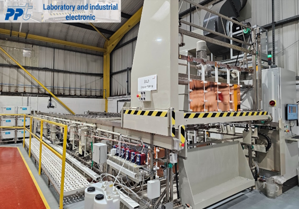 Merlin Flex have successfully installed and commissioned their new Copper Panel Plating Line. The new line, supplied by PPT in Slovakia, replaces their previous line originally installed back in 1991. The PPT panel plating line provides copper plating capabilities for very thin flexible panels plus flex & Flex/Rigid panel lengths. Read More » Merlin Flex have successfully installed and commissioned their new Copper Panel Plating Line. The new line, supplied by PPT in Slovakia, replaces their previous line originally installed back in 1991. The PPT panel plating line provides copper plating capabilities for very thin flexible panels plus flex & Flex/Rigid panel lengths. Read More » |
| Teledyne Labtech | 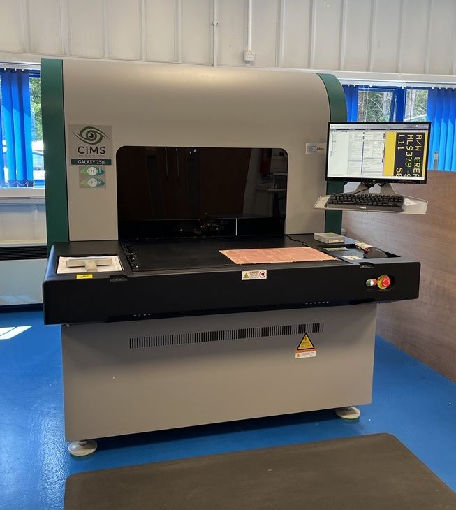 Teledyne Labtech is excited to announce the installation and commissioning of our new CIMS Galaxy 25µm AOI, supplied by Adeon Technologies. Capable of inspecting HDI and multi-layer PCB with min line/space down to 25µm. Read More » Teledyne Labtech is excited to announce the installation and commissioning of our new CIMS Galaxy 25µm AOI, supplied by Adeon Technologies. Capable of inspecting HDI and multi-layer PCB with min line/space down to 25µm. Read More » |
| Polar Instruments |
Many customers have asked for readings of insertion loss at specific frequencies to be added in the Si9000e user interface in order to facilitate specifying Delta-L or SPP or other loss method testing. The latest Si9000e does just that – the insertion loss results at user nominated frequencies are now displayed alongside the All Losses plot. For details, along with all the other recent enhancements please follow this link to this presentation. Read More » |
| Go back to Contents |
Membership News |
||||||||||||||||||||||
|
|
New Members
|
|||||||||||||||||||||
| Go back to Contents | ||||||||||||||||||||||
ICT Council Members |
|
|
Council Members |
Emma Hudson (Chair), Andy Cobley (Past Chairman), Steve Payne (Hon Deputy Chairman), Chris Wall (Treasurer), William Wilkie (Technical Director, Hon Sec, Membership & Events), Richard Wood-Roe (Journal Editor & Web Site), Jim Francey, Martin Goosey, Lynn Houghton, Pete Starkey, Francesca Stern and Bob Willis, |
Editors NotesThe ICT Journal |
|
|
Richard Wood-Roe |
Instructions / Hints for Contributors 1. As it is a digital format the length is not an issue. Short is better than none at all! 2. Article can be a paper or a text version of a seminar or company presentation. Please include data tables, graphs, or powerpoint slides. We can shrink them down to about quarter of a page. Obviously not just bullet points to speak from. 3. Photo's are welcome. 4. We would not need source cross references 5. Title of presentation - Of course! Date, Job title of Author and Company represented. 6. An introductory summary of about 150 words would give the reader a flavour of what it's all about. 7. Style - we don't want out and out advertising but we do recognise that the author has a specialism in the product or process that will include some trade promotion. Sometimes it will be a unique process or equipment so trade specific must be allowed. 8. Date and any info relating to where or if this article may have been published before. 9. We can accept virtually any format. Word, Powerpoint, publisher, PDF or Open Office equivalents. 10. Also, to make it easy, the author can provide a word file to go along with his original powerpoint presentation and I/we can merge it together and select the required images. 11. A photo of author or collaborators. I really do look forward to receiving articles for publication. Richard Wood-Roe |