|
The Journal of |
| Section 1 | Editors Introduction |
|
Richard Wood-Roe |
In this issue of The Journal our first paper is fom Atotech and outlines the lessons learned while investigating microvia failures. There is a thorough review of the examination techniques and the recommended assessment procedures used. Our second paper is from Resonac Group of Japan and describes the development of a low loss adhesive film for bonding multilayer PTFE substrates. Finally we have a paper outlining the latest developments of laser drilling using high frequency burst mode from The Applied Laser Photonics Group and Schmoll Maschinen Pete Starkey has provided an excellent review of our Christmas symposium at Harrogate. I have found a generous amount of items to add to the industry and membership news sections. Our future events include the spring seminar in March and the popular Foundation Course which will will be in April this year at Chester University. I hope you find the contents of the Journal interesting. I welcome your input for the next edition. |
| Go back to Contents |

| Section 2 | Calendar of Events | |
Bill Wilkie |
2024 |
Details |
| March 5th |
ICT Spring Seminar and AGM on 5th March 2024 At the Manor Hotel, Meriden The AGM this year involves the election of a Chairman and Vice Chair. Nominations are invited for these posts and also for the election of new Council Members. |
|
| April 15-18th |
Annual Foundation Course on 15th - 18th April 2024 The Foundation Course will be held at Chester University, with the first day hosted by the Merlin Group at their Deeside facility. |
|
| Go back to Contents | ||
| Section 3 |
Paper 1 |
|
Lessons Learned While Investigating Microvia Reliability Failures. Tobias Bernhard, Roger Massey, Senguel Karasahin, Frank Brüning |
|
 Dr Tobias Bernhard Dr Tobias BernhardResearch Scientist Atotech Deutschland GmbH |
Abstract. Over the last few years, there has been a slow, but increasing number of reports concluding that stacked micro vias are failing preferentially when compared to an alternative staggered via design. However, while a staggered interconnect arrangement could be seen as a solution to satisfy the reliability demands, they are usually undesirable as they consume larger amounts of real estate which can’t be tolerated in many applications. With strong evidence available, the preferential failure of stacked micro vias can’t be denied, and as such, there is now a growing number of investigations ongoing to examine microvia reliability and determine if and why staggered micro vias fail preferentially, and also trying to identify what is the ideal microvia structure for best reliability performance. As part of investigations into microvia failures, we review the published data and find that while these new analysis tools are being readily used, there is what we consider to be some misinterpretation of the data, leading to inaccurate route cause diagnosis, and conclusions that are questionable at best, or wrong and misleading at the worst. This paper summarizes these initial investigations and discusses the misinterpretation of data as well as offering some insight into other microstructural characteristics which will likely impact the physical properties and reliability of plated blind micro vias.
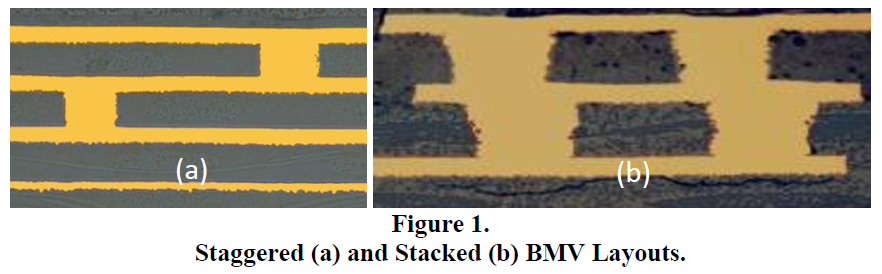
As with all production processes, there is a learning curve, in-which, products are initially prone to increased production variances, which lead to performance and quality issues, and as is normal, these diminish over time until a high volume, high reliability process is established. Laser drilled BMVs have undergone such a cycle, with BMVs generally now being considered as a robust interconnect method. As mentioned previously, stacked BMVs are often preferred by product designers as they utilize not only a smaller footprint, enable higher track densities with smaller pad pitch, but also allow for enhanced thermal paths which are also a necessity in many modern electronics units where, heat flow can be as critical as electrical flow. One ongoing concern with stacked BMVs is the impact arising from heat, namely the expansion which occurs during PCB assembly as well as once those populated PCBs reach their final service application. With a series of stacked BMVs being essentially a “solid” column of Copper, the thermo-mechanical properties of the BMV stack is dramatically different to that of the surrounding dielectric matrix, and so there is understanding that significant stresses can arise at the interfaces between each individual via as well as between the complete stack and its encapsulating glass/epoxy resin. While this concern has always existed, and it has been proven to exist, where there have been concerns for final product reliability, it has been found that a staggered BMV pattern can accommodate the applied thermal strains and offer an improved product lifetime, and so have been adopted. Unfortunately, with modern electronic applications demanding the highest possible densification in the smallest possible area, the use of staggered BMV designs is becoming unacceptable and the need for a high reliability stacked BMV design is re-emerging. It must be pointed out however, that stacked BMVs are very widely used within many of today’s PCB designs without excessive field or assembly failures, however, there are increased reliability applications such aeronautics, space and military, where there is a rapidly growing concern over the long term reliability of stacked BMVs. It is fair to say that while this concern has been steadily increasing, it has been predominantly within those users located in the USA, however, with many PCB users and producers now having a presence and operations in many countries, this concern has begun to spread and has become more of a global issue than it has been in the past. In mid-2018 IPC released a white paper[1] which as its name implies raised a “call to arms” among the PCB industry as a whole, to review the performance of BMVs, and since that time, there have been an increasing number of papers at technical conferences reiterating and highlighting the need to investigate BMVs further.[2] This paper, summarizes a number of investigation techniques used when examining failures occurring within stacked BMVs following thermal screening, or during field service, and highlights the need for the correct analytical tools to be used otherwise there is a risk of root cause being incorrectly identified.
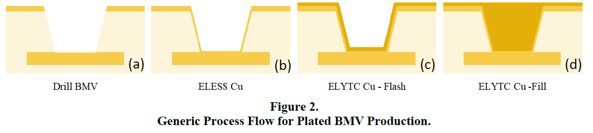
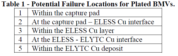
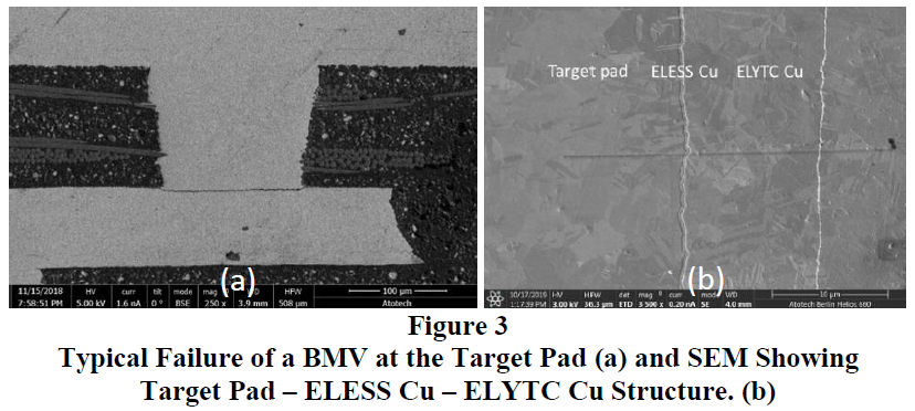
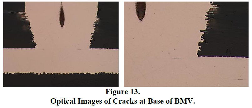
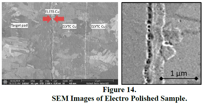
In terms of failures exhibited by BMVs, the most commonly reported is one referred to as capture, or target pad separation, an example of which can be seen in Figure 3a. For such failures, it is typically found that the failure occurs at the base of the BMV where the plated deposit connects with the previously formed target pad. From Figure 2 it is clear that this target pad to plated layer interface is a complex structure comprising of the target pad itself, underlying an electroless Copper (ELESS Cu) or other metallization layer, which is then covered with an electrolytic plated Copper (ELYTC Cu) layer, (Figure 3b), as such, it can be appreciated that there are multiple potential locations for failure. (Table 1)
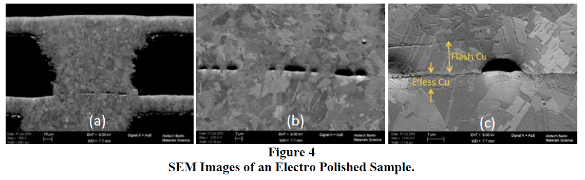
Typical Investigation Techniques. Electro Polishing.
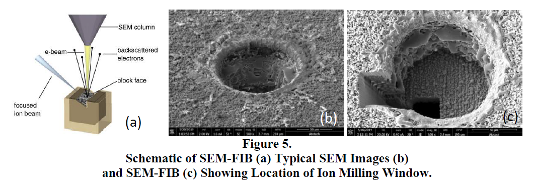
From Figure 4a and 4b it is clear that there is a line of voids at the base of the BMV, what is not known however, is the exact location of those voids, namely do they occur at the target pad – ELESS Cu interface, within the ELESS Cu layer itself, at the ELESS Cu – ELYTC Cu interface, or within the bulk plated Cu? This knowledge is essential in understanding the root cause of the defects, and identifying the process area in need of troubleshooting activities. Following the electro polishing operation, it becomes possible to distinguish the boundaries where the target pad, ELESS and ELYTC Cu layers occur. In view of this, in Figure 4c, it is clear that the line of voids occur not at the target pad – ELESS Cu interface as is often assumed, but actually at the ELESS Cu – ELYTC Cu interface. Scanning Electron Microscopy with Focus Ion Beam. In order to open up such an inspection window in the sample, an incidental ion beam is used to “mill” or ablate material, and through automated scanning of the ion beam, a high level of control can be achieved, enabling detailed penetration into the sample.
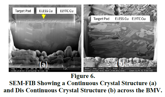
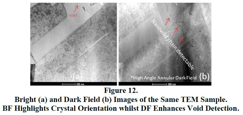
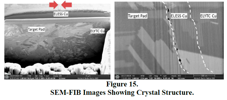
One of the first points typically noted during FA of BMVs is the general crystal structure within the plated Copper, and this generally falls into 2 distinct groups. The first showing a single uniform crystal structure where the interface between the target pad and the plated Cu cannot be distinguished (Figure 6a), or a structure where there is a break in the crystal continuity and one or more clear interfaces can be seen (Figure 6b) While, it could be argued which of the two structures would offer the “best” reliability performance, it is offered that a single crystal pattern would be preferential, as any marked changes in crystal structure would generally enable some form of stress concentration, and could exacerbate failure. It should also be considered, that such changes in structure typically occur around the target pad – ELESS Cu – ELYTC Cu interfaces, and as this is commonly the point of BMV failure, it would be sensible to propose that a continuous metallography would be desirable. Such structures arise due to the crystallization of plated deposits that occurs following plating. Immediately after deposition the plated layer has no defined crystal structure, but will begin to develop one over a period of time, ideally this recrystallization occurs in a “bottom up” fashion, with each new layer following the crystal orientation of the underlying layer, i.e. the ELESS Cu continues the orientation of the target pad Cu, and then the ELYTC Cu follows the orientation of the ELESS Cu layer. Known as epitaxial growth, this process occurs naturally, although it should be acknowledged that there are influences within the process and the chemical constitution of the plating chemistries which can impact the recrystallization characteristics of plated layers. While optical microscopy and SEM, in combination with etching processes will enable inspection of a BMV crystal structure, SEM-FIB is becoming a popular means to achieve this as, once the ion milling has opened the inspection surface, there is no need for secondary etching and there is minimal risk of over or under etch leading to ambiguous results.
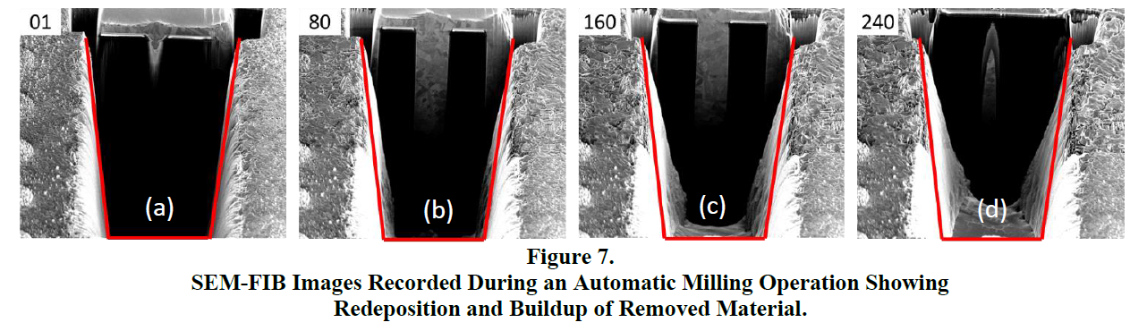
Possible Mis-Categorization with SEM-FIB. One point to consider, and is often overlooked, is the removal of the sample material itself during the “cut” or milling operation, and where that material goes once it has lifted from the sample. As with all SEM units, there is a series of vacuum and detector systems that remove and make use of these “sample” streams, yet the volume of material removed during a FIB- cut is substantially higher than that created when performing simple elemental analysis, yet it is assumed that the operating vacuum and exhaust system in the SEM chamber is sufficient to accommodate this high material removal rate, yet this is not necessarily the case. Figure 6 shows a prepared SEM-FIB sample, where the initial “cut” has been made manually in order to approach a Copper filled Through Silicon Via (TSV) Once the TSV has been reached, the automatic milling and serial imaging process was begun. During this automatic operation there are two major points of note. 1. As expected, the Cu filled TSVs become revealed as the cut proceeds through the sample
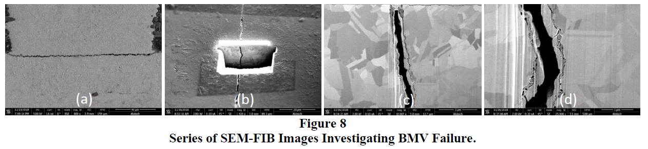
It is point 2 that is of most interest as this material build up contains the plated Cu from within the TSV itself. As such, it is a redeposition of the material removed during the cut or milling operation. For the images shown, the redeposition was not considered an issue as it did not impact the investigation being made, as there were no structural defects within the TSV itself, but when such a technique is used to investigate a cracked BMV, there is a serious cause for concern. The primary requirement during FA is that the techniques used do not influence, or change the sample being inspected, otherwise there is a strong likelihood that the collected data can be misleading. If material redeposits on the sample during a FIB-SEM investigation then this primary requirement is broken, and the conclusions drawn from the analysis must come under question. In the case of a cracked BMV, there is a very high likely hood that the redeposition will occur not only within the milling box but within the crack under investigation, in view of this, the crack may appear to be coated with Cu which can be mis-interpreted as a defined layer or coating. Figure 8 shows a series of SEM-FIB images taken while investigating a failed BMV joint, clearly the point of failure is located at the base of the BMV and it would be reasonable to anticipate that it would be located close to, or cognizant with one of the target pad – ELESS Cu – ELYTC Cu junctions. Through the use of an automated milling procedure, an inspection plane normal to the crack has been created. In Figures 8c and 8d there appears to be a distinct layer of material on either side of the failure crack, and when measured, this is found to be approximately, 1um in thickness, which is comparable to that of the deposited ELESS Cu layer. As such it would be reasonable to conclude that the crack arose due to cohesive failure within the ELESS Cu layer as this can be clearly seen on either side of the crack surface.
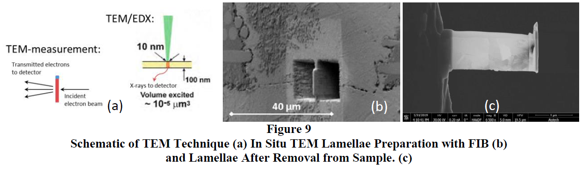
Transmission Electron Microscopy. As the name, suggests, TEM is a transmission method, meaning that the detectors are typically positioned beyond the sample, and they collect particles following their transport through the sample, unlike SEM where the detectors are commonly in front of the sample and collect particles that have been scattered, reflected or emitted off the sample surface. TEM does require specialist sample preparation, typically involving SEM-FIB to cut a thin lamellae which can then be examined transmissibly. (Figure 8)
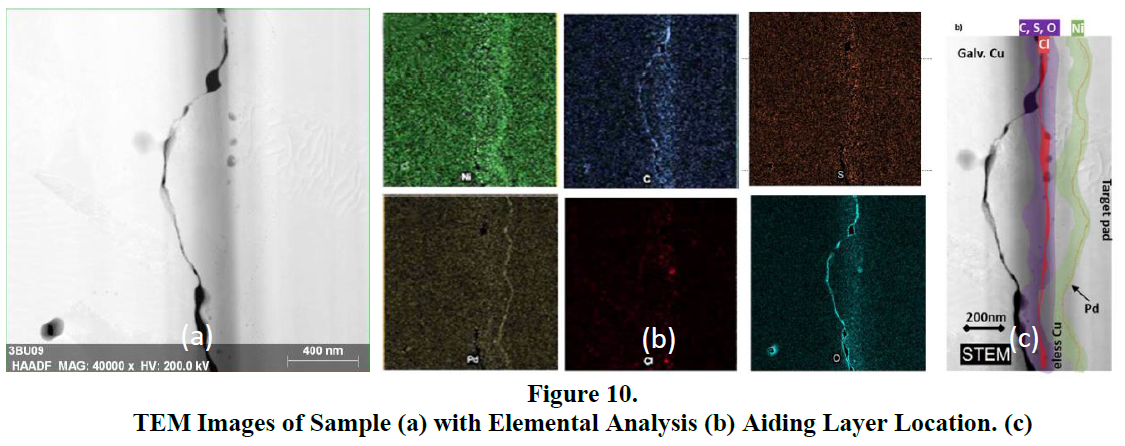
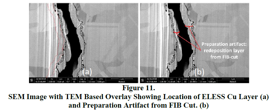
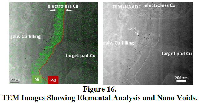
If we now refer back to the example in Figure 8 where the BMV failure is attributed to cohesive failure within the ELESS Cu layer. Through TEM analysis, we can now determine the location of the ELESS Cu layer itself, which, as shown in figure 11b, is found to be not only wholly intact but located to the left side of the crack, implying that the material found on the inner faces of the fracture surface are in fact redeposited artifacts arising from the FIB cut. In view of this, it can now be concluded that the BMV failure itself could be associated with adhesive failure between the ELESS Cu and ELYTC Cu layers.
We have reported elsewhere[3,4,5] on the presence of nano voids found during TEM-DF investigations, and this has led to a unique and increased understanding on potential failure mechanisms for BMV structures, but has importantly also enabled us to offer a “best practice” process for similar investigations. Suggested “Best Practice” for BMV Failure Inspection. It should be noted that investigations of separated joints with visible cracks is not recommended, due to preparation artefacts from cross sectioning and the high potential for redeposition layers forming during ion milling operations with SEM-FIB. However, if this is not possible, care should be taken to ensure that such artefacts do not lead to misleading conclusions.
References Previously published in IPC Expo proceedings |
| Go back to Contents |
| Section 4 |
Paper 2 |
|
Development of Low Loss Adhesive Film for Multilayer PTFE Substrates |
|
|
Yusuke Watasa Resonac Group |
Abstract Introduction
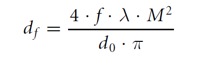
Formulas 1 and 2 show that the higher the frequency, the greater the loss, so an adaptation to high frequency is essential in millimeter wave band applications. Therefore, it is required to use a low dielectric material as the insulating substrate material.
|
| Go back to Contents |

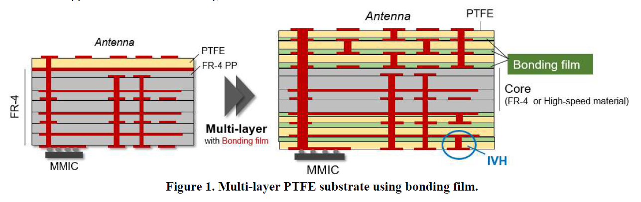
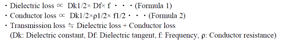
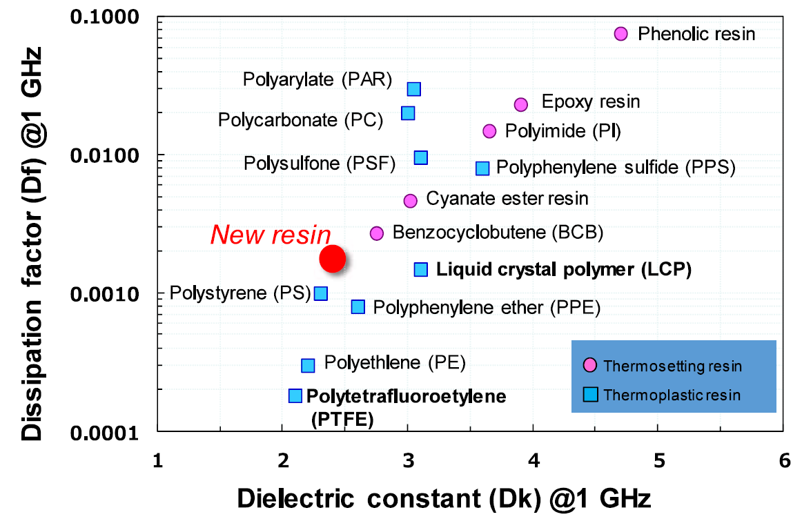
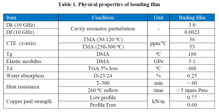
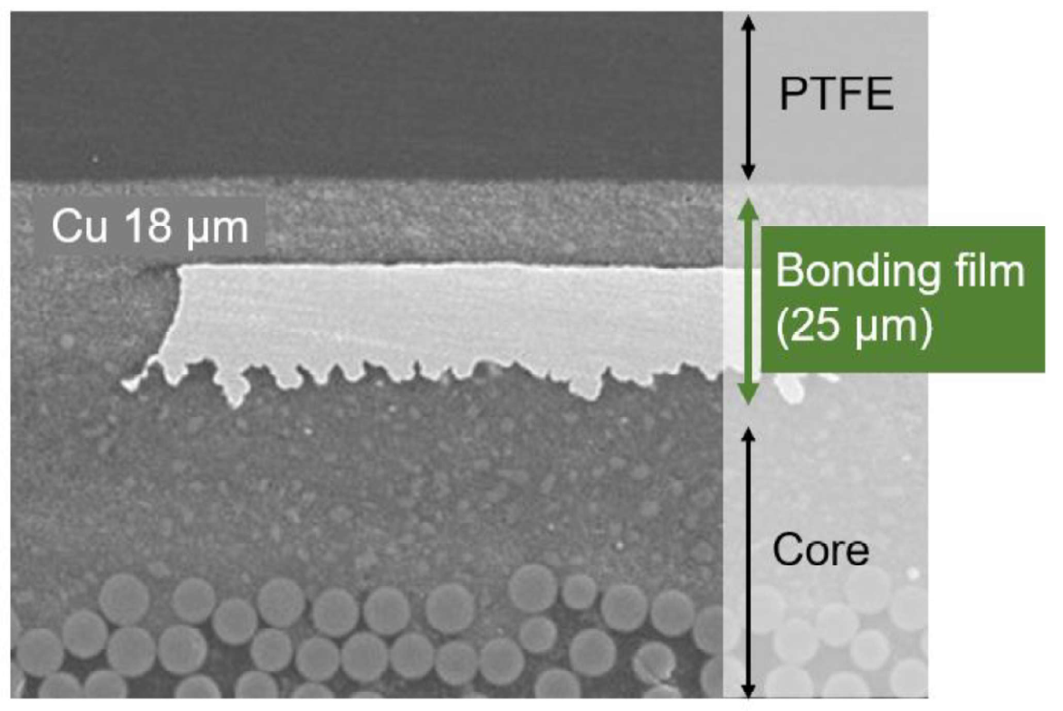
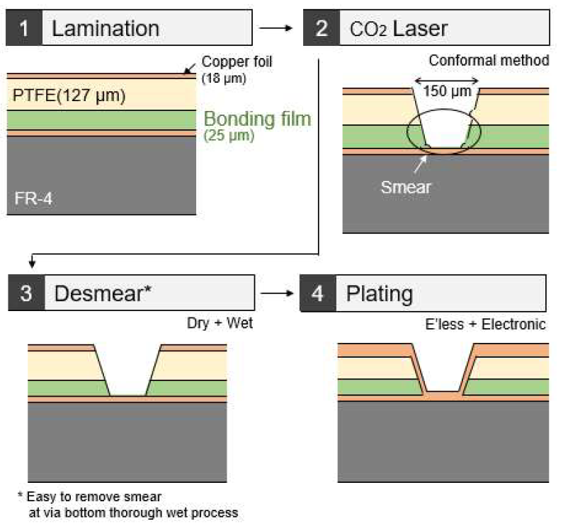 Figure 4. Via fabrication process of PTFE substrate with novel resin.
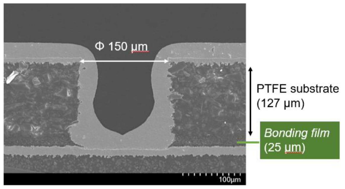
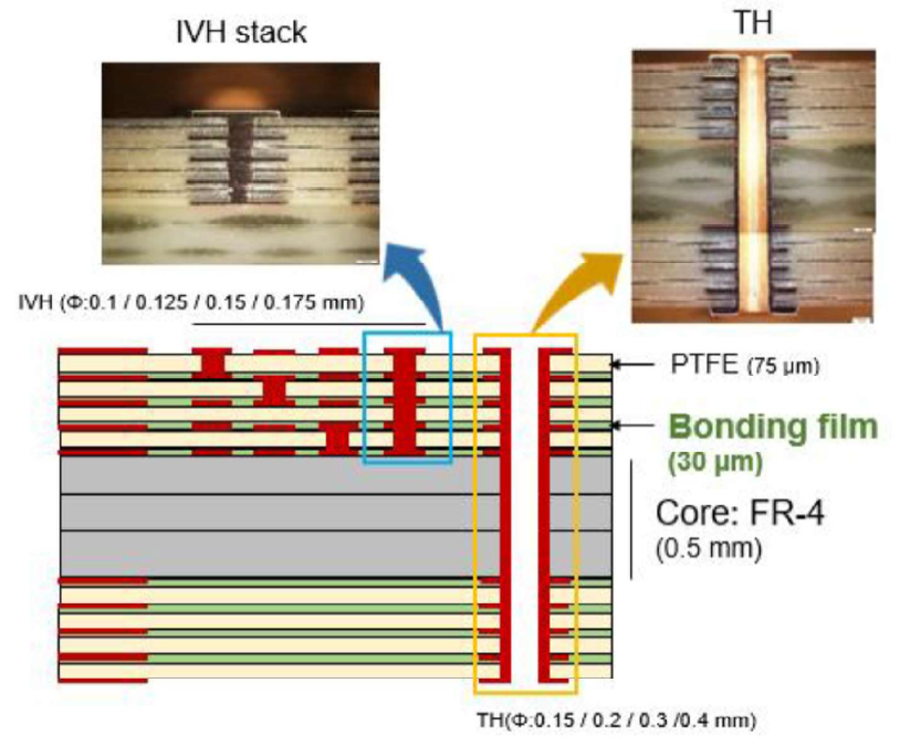 Figure 6. Cross-section of multilayer PTFE substrate.
| Section 5 |
Paper 3 |
|
|
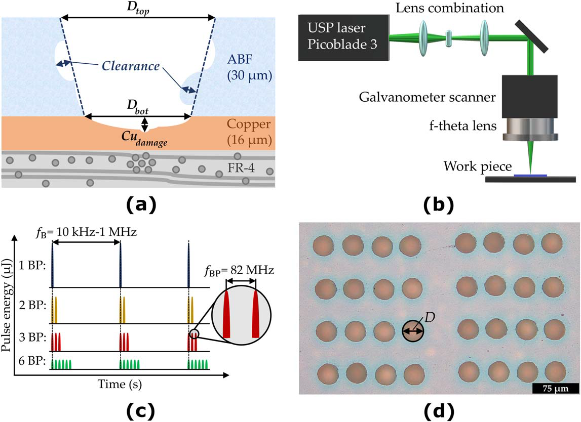
Picosecond Laser Microvia Drilling of ABF Material Using MHz Burst Mode Daniel Franz1 , Tom Häfner2, Kay Bischoff1, Jonas Helm1, Tim Kunz2, Stefan Rung2, Cemal Esen3 and Ralf Hellmann1 |
||
|
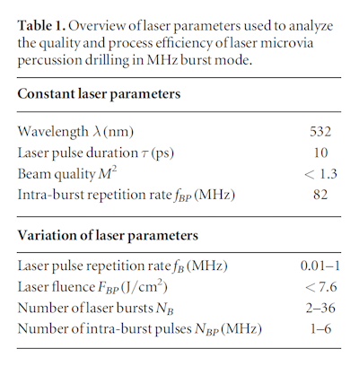
Abstract We report on a comprehensive study of laser percussion microvia drilling of Ajinomoto build-up film (ABF) material using an ultrashort pulsed laser in MHz burst mode. After laser processing, microvia drilling quality is was evaluated by observing the fabricated diameter and taper using laser scanning microscopy and metallography. The influences of the incubation effect, heat accumulation and shielding effects as a result of pulse to pulse interactions are assessed on the ablation threshold, penetration depth and laser microvia drilling quality. We found that an increasing heat accumulation in MHz burst mode processing is responsible for the void formation and delamination of the insulating ABF layer. Therefore, the parameter clearance was introduced to evaluate these effects on the microvia sidewalls. For a comparable clearance, applying 2 intra-burst pulses achieves an average reduced taper of down to 19.5% compared to single pulse mode. At the same time, a reduced laser drilling time of 16.7% per microvia highlights the enormous potential of the MHz burst mode for laser drilling of ABF material in printed circuit board fabrication. 1. Introduction The trend towards miniaturized high-performance electronic components driven by increasing demands on their functionality requires a high-density electronic packaging and interconnection technology. Hence, laser drilling has been intensively studied for various materials used in interconnect devices, such as, e.g., ceramics or different printed circuit board (PCB) materials[1–6]. In particular, ultrashort pulsed (USP) laser percussion drilling has been established for the fabrication of blind vias, so-called microvias, to inner conductive layers in multi-composite PCB material[5-8] with small diameters of <10 μm[9-10]. To ensure reliable electrical interconnections with a high thermal durability, the capture pad should be spatially exposed as much as possible, typically in a range of 70%–90% with respect to the upper microvia diameter[11]. In addition to the most common printed circuit board substrate FR-4, an epoxy resin filled with spherical glass particles called Ajinomoto build-up film (ABF) material is gaining interest as an insulating layer[7-11,14]. A USP laser enables material ablation with small focal diameter and negligible thermal stress due to its short laser pulse duration in the picosecond and femtosecond range[8-15]. Characteristic nonlinear absorption mechanisms are the result of very high pulse peak intensities of above 1013–1014 W/cm2[16-17], allowing an absorption of even transparent materials such as polymers and glasses[18-19]. The tremendous interest and potential of USP lasers has led to the ongoing development of high average powers. 1kW and more are nowadays available for laser micromachining.[20-23] Consequently, the arising laser pulse energies of up to some 100 μJ lead to a laser fluence that is significantly above the well-known optimum for maximizing the ablation efficiency and rate[24]. For scaling the laser pulse energies closer to the optimum ablation efficiency, so-called laser burst mode can be used to split a laser pulse into at least two and typically up to a few hundred intra-burst pulses with a temporal intra-burst interval in the nanosecond range.[24-31] However, within the timescale of a few nanoseconds between successive intra-burst laser pulses, several pulse to pulse interactions occur and their significant influences on processing efficiency and quality in laser micromachining have to be considered[6,32-38]. Even with ultrashort laser pulses, a fraction of the laser pulse energy remains in the substrate as heat during the ablation process[26,36]. Heat accumulates over time if the time interval between successive laser pulses is insufficient to dissipate the induced heat into the surrounding material, which in turn is limited by the material-specific thermal conductivity[37,39]. Furthermore, Several studies and simulations of laser drilling of metals[28,41,44], dielectrics[45] and glasses[46-47] have reported improved ablation efficiency, ablation rate, ablation volume, penetration depth and drilling quality as a consequence of using laser bursts in the MHz regime. The results are mainly attributed to heat accumulation and are discussed in terms of laser-induced shielding effects by plasma or ejected particles and incubation effects as a result of pulse to pulse interactions of successive intra-burst laser pulses. In contrast to these studies on laser drilling of single component materials with USP lasers in MHz burst mode, the effects of pulse to pulse interactions in laser drilling of multi-composite materials such as ABF material for PCB fabrication have not yet been investigated. Hence, the aim of this study is to fundamentally understand the impact of pulse to pulse interactions in laser percussion drilling of ABF substrate with MHz bursts on the ablation threshold, penetration depth as well as drilling quality of microvias. Therefore, bore craters were generated into ABF material under various MHz burst configurations and evaluated by laser scanning microscopy and metallography.
Experimental investigations of laser microvia percussion drilling in ABF material were performed using a high-power USP laser (Lumentum, Picoblade 3) with a laser pulse duration of τ = 10 ps, a wavelength of λ = 532 nm and a beam quality of M2 < 1.3 in MHz burst mode. In all experiments, GX-T61 ABF PCB material with a layer thickness of 30 μm and a 16 μm thick inner copper layer was examined, see figure 1 (a).
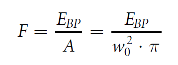
Equation 1 The study evaluates the ablation behavior of ABF material and copper as well as the laser microvia drilling quality using a number of intra-burst pulses of NBP = 1–6 and an intra-burst pulse repetition rate of fBP = 82 MHz (consequently a time interval between successive pulses of ΔtBP = 12 ns), see figure 1(c). For each bore crater, both the total energy input and the intra-burst pulse energy distribution was maintained constant. Therefore, the pulse energy in MHz burst mode has been set accordingly by adjusting the gain factor of each intra-burst pulse. For example, to compare the results with a single pulse mode (1 intra-burst pulse) at a laser pulse energy of EBP = 30 μJ, the laser pulse energy is reduced to EBP = 10 μJ using 3 intra-burst pulses. First, the damage threshold method based on Liu[49] is used to determine the ablation thresholds of GX-T61 ABF material and pure copper material with a sample thickness of 500 μm at a laser burst repetition rate of fB = 10 kHz and 1 MHz with laser fluences of up to 7.6 J cm−2 and a number of laser bursts of NB = 15. To evaluate the ablation threshold of the PCB materials, first the laser fluence FBP is calculated according to equation 2. Equation 2 Where EBP is the laser pulse energy and w0 the radius of the beam waist (1/e2) [6]. The logarithmic representation of the squared drilling radii generated as a function of the laser fluence is then used to determine the material-specific ablation threshold Fth.
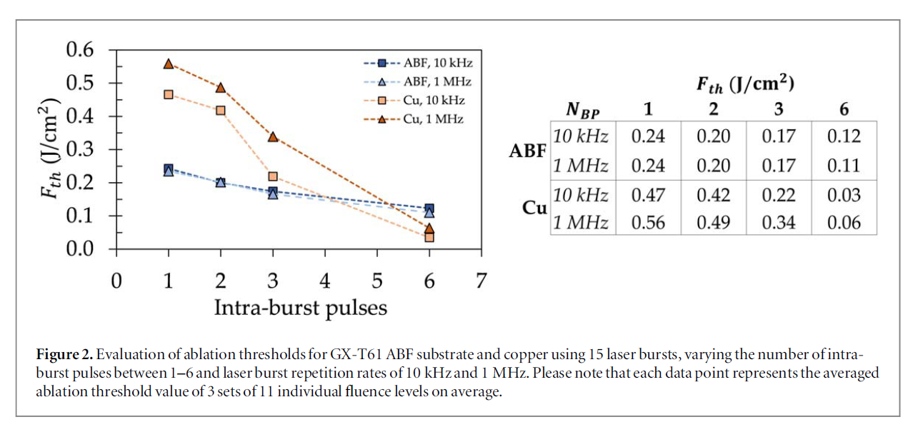
3. Results and discussion 3.1. Ablation behavior in MHz burst mode 3.1.1. Ablation threshold. In order to evaluate the potential of picosecond laser pulses in MHz burst mode for percussion drilling of microvias into PCB material, firstly, a fundamental characterization of the ablation behavior of processes involved and materials is mandatory. Hence, the ablation thresholds of GX-T61 ABF material (dielectric layer) and pure copper (conductive inner layer) are determined.
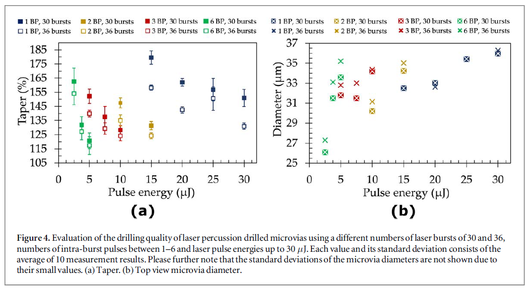
3.1.2. Penetration depth, diameter and ablation volume. The ablation volume, penetration depth and diameter were determined using laser scanning microscopy in increments of two laser bursts. The averaged results are shown in figure 3 for a sample size of 3, a number of intra-burst pulses of NBP = 1–6 and a laser burst repetition rate of fB = 200 kHz.
An overview of top view images of percussion drilled microvias into ABF material in increments of 2 laser bursts in dependence of the number of intra-burst pulses is provided in figure 3(a). It is clearly visible that for applying the same total energy, the inner copper layer is reached with fewer laser bursts for MHz burst mode in comparison to single pulse mode. The evaluation of the penetration depth as a function of the number of applied laser bursts and intra-burst pulses is depicted in figure 3(b) and reveals that the 30 μm thick ABF insulating layer is drilled through by using 18 laser bursts for single pulse mode. In contrast, applying a number of intra-burst pulses of NBP = 2, 3 and 6 intra-burst pulses, only 16, 14 and 12 laser bursts, respectively, are required to reach the inner copper layer. From this point of view, throughput in PCB fabrication can be improved by reducing the laser microvia drilling time of 16.7%–33.3%. It is also worth noting that after reaching the conductive layer in MHz burst mode, the penetration depth in copper is not affected and is comparable to that in single pulse mode. 3.2. Evaluation of the microvia drilling quality
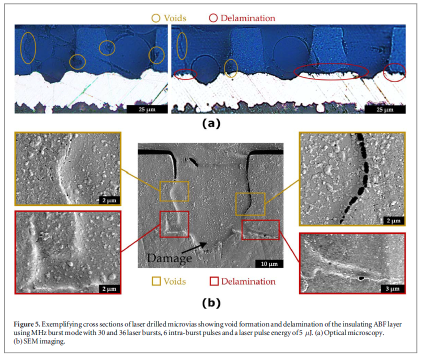
3.2.2. Clearance of microvia walls. Although the laser drilling quality is improved by accumulated heat using MHz burst mode, negative side effects occur. Voids are created and even delamination of the insulating ABF layer is observed for 6 intra-burst laser pulses. For illustration, selected cross sections of laser drilled microvias with 30 and 36 laser bursts and a number of intra-burst pulses of 6 are shown in figure 5 using optical microscopy and SEM imaging.
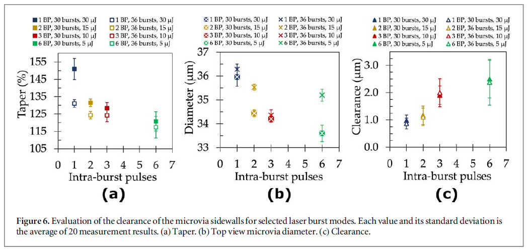
Since the formation of voids can lead to a significant reduction of the electrical connection lifetime after electroplating by more than 90% [59], a characterization of the voids is indispensable. Hence, the previously introduced parameter clearance is used to evaluate the size of these modifications, figure 1(a). This parameter is also retained to quantitatively describe the effect of accumulated heat when using MHz bursts.
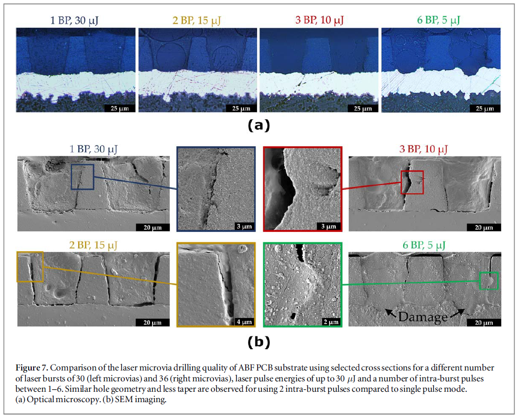
from figure 4 and additionally depicted in figure 6(a) and (b). Obviously, the clearance is independent of the selected number of laser bursts of NBP = 30–36, but increases continuously with the number of intra-burst pulses, reaching highest averaged values of 2.44 ± 0.76 μm for 6 intra-burst pulses. Compared to the single pulse mode with small clearance values of 0.93 ± 0.2 μm, the values are doubled with 1.96 ± 0.43 μm for 3 intra-burst pulses and in a comparable range with 1.16 ± 0.3 μm for 2 intra-burst pulses. From this point of view, the evaluation of the clearance represents well the evolution of the voids with an increasing number of intra-burst pulses. This is also in good agreement with selected optical microscope images and SEM images of microvia cross sections shown in figure 7.
4. Conclusion Acknowledgments References Editors Note This paper is licensed by Open Access 4.0. It is published in full with no modifications. https://creativecommons.org/licenses/by/4.0/ |
||
| Go back to Contents |
| Section 6 |
The Institute of Circuit Technology Christmas Seminar 2023 December 5th 2023, Harrogate |
 ICT Chair ICT Chair |
A multitude of delegates from the UK printed circuit industry made the journey to the Institute of Circuit Technology Christmas Seminar on December 5 at the grandiose Majestic Hotel in the picturesque spa town of Harrogate in North Yorkshire. They were welcomed by ICT Chair Emma Hudson, who introduced a program of three presentations encompassing the diverse topics of satellites, electroless metallisation and electronics manufacturing initiatives. |
 |
“The next industrial revolution isn’t on Earth” is the tagline for Space Forge, a British aerospace manufacturing company developing fully reusable satellites designed to take maximum advantage of the unique environmental benefits of space in manufacturing next-generation super-materials. Darren Cadman introduced the company and its strategy. He described Space Forge as Europe's fastest-growing space-tech start-up, with funding from the UK Space Agency and the European Space Agency, together with several international investors. The company’s objective is to establish a microgravity research center to drive advanced material research and production, primarily focused on growing defect-free inorganic crystal structures in microgravity conditions for use in electronics. The huge demand for such a service is currently not being met. Not only is there a heavy reliance on the International Space Station but there is a lack of both a dedicated platform and a cost-effective soft-return mechanism. The key attribute of Space Forge is its world-first reusable, returnable orbital manufacturing platform, with its patented system to enable re-entry without burning up and a subsequent soft landing to protect fragile payloads, while reducing stress on the vehicle and minimizing the cost of refurbishment in preparation for re-launch. Cadman explained that in-space manufacturing offers unique environmental benefits that can facilitate the creation of large, near-perfect crystals by chemical vapor deposition and enable the production of semiconductor products with performance superior to anything that can be achieved on Earth, where defects can result from gravity, causing buoyancy effects and preventing perfect mixing of gases, solutions or alloys of different densities. Furthermore, atmospheric contamination issues are avoided in space, where ambient pressure is 10 trillion times lower, and temperatures close to absolute zero can be achieved by radiators facing cold space with no need for cryogenics. The Space Forge manufacturing platform is designed to be launched to a low-Earth orbit at a height of 550 km, with a three-month operational phase followed by a precision de-orbit and recovery from the sea, then taken back to base for inspection of vehicle and payload, refurbishment, and return to service. The system has the potential to prevent the generation at least 15 tons of carbon dioxide for every kilogram of semiconductor material produced for next-generation electronics, telecommunications and automotive applications. |
 |
Next to speak was Andy Cobley, professor of electrochemical deposition and leader of the functional materials research group at Coventry University, discussing the development of non-noble metal activators for electroless plating processes, in a project carried out in collaboration with Université de Mons in Belgium. Reviewing the history of electroless copper plating in the electronics industry, Professor Cobley commented that its capability to metallise non-conductive materials has established it as an enabling technology in printed circuit manufacture and latterly in the rapidly evolving field of electronic textiles. Electroless deposition requires the non-conductive surface to first be treated with a “catalyst,” an activator that initiates the redox reaction whereby copper is reduced from the ionic state in solution and deposited on the surface as metal. Formaldehyde is typically used as the reducing agent, and subsequent deposition of copper proceeds autocatalytically. The catalyst of choice has traditionally been colloidal palladium. But palladium is scarce, much in demand, and currently priced at more than £25,000 per kilogram, justifying the evaluation of lower-cost alternatives. Using palladium as a baseline, screening tests were carried out on three candidate materials: titanium dioxide, zinc powder, and cobalt powder. A polyester textile was used as the substrate. Professor Cobley explained the experimental procedure and summarized the results in terms of the effects of concentration, immersion time, temperature, dispersion method, and particle size. He used a series of SEM micrographs to illustrate the physical differences in deposit characteristics. It was observed that both zinc and cobalt could initiate the electroless copper process, and the dispersion method and particle size has significant effects on the final properties of the copper deposit. However, the initiation mechanism was found to be different from that of palladium, since neither zinc nor cobalt showed any catalytic activity. In contrast, palladium acted as the catalyst in oxidizing formaldehyde resulting in copper from solution being reduced to form the initial metal deposit upon which subsequent copper was deposited by autocatalytic reduction. In the case of zinc and cobalt, the initial copper deposit was formed by a simple displacement reaction by a metal lower down in the electrochemical series. |
 |
The final presentation came from Steve Payne, project manager at iNEMI, the international electronics manufacturing initiative with a mission to be the premier collaboration forum to forecast and accelerate improvements in the electronics manufacturing industry. He explained the structure of iNEMI, its high-profile global membership, and how its roadmap identifies, forecasts, and prioritizes the future technology requirements, evolution, and infrastructure of the global electronics manufacturing industry in terms of applications and market drivers, technical needs, maturity of technical solutions and expected gaps and challenges—all with a 10-year outlook. He described how individual roadmap teams focus on the full lifecycle and ecosystem of a product, from design through manufacturing and operation to end-of-life, leveraging resources across the supply chain and collaborating to address common industry knowledge gaps. Payne reviewed the portfolio of current iNEMI projects, highlighting those with particular relevance to printed circuit fabrication issues, and described in some detail the work on reliability and loss properties of copper foils for 5G applications, with particular reference to the surface treatment processes used to improve adhesion to resin systems and their effect on signal loss and integrity at high frequencies. Specific objectives were to: Determine and characterize the best non-contact method for measuring the surface topography of very-low-profile copper foil finishes 1. Establish consistency in specifying surface topology of copper foil and bonding treatments
Electrodeposited and rolled-annealed foils were included in the program. Payne briefly discussed non-contact roughness measurement and explained the different parameters: Sa: Representing average surface roughness The current phase of this program is the fabrication of microstrip circuits for the correlation of signal loss with surface conductivity. The next step will be reliability testing, looking for better information than could be gained from traditional peel testing. Other current iNEMI projects mentioned by Payne were: PCB characterization for CAF and ECM failure mitigation, hybrid PCBs for next generation applications, and the PCB connector footprint tolerance project. PCB initiatives in development include immersion cooling, embedded components, ultra-HDI challenges, halogen-free laminate flame retardancy challenges, PCB-level optical interconnects, and pad cratering mitigation. Payne’s presentation certainly captured the attention of the audience and initiated an energetic Q&A session, capably moderated by Hudson, which continued through the buffet supper and into the hotel bar, where it metamorphosed into a welcome networking opportunity for PCB people. Pete Starkey, I-Connect007 |
| Go back to Contents |
 Graphic PLC are pleased to announce Anthony Jackson will be joining our Engineering team. Anthony has many years of experience within the industry, we look forward to working with him and welcoming him to the Graphic family!
  Taiyo America, Inc. is happy to announce that Stuart Down, EMEA sales manager has been elected as EIPC Board Member 2024-2025!
|
Industry News |
|
| A-Gas |
To assemble the list, TIME's editors and reporters fielded nominations and recommendations from industry leaders and partner organisations, like Global Optimism and The B Team, as well as TIMECO2’s (the climate arm of TIME) Advisory Council, then worked to assess the candidates on a variety of factors, including recency of action, measurable results, and influence. Read more...... |
| Adeon |
It is with enormous pride that Adeon Technologies can announce it has received multiple purchase orders from Teltonika from Vilnius, Lithuania for supplying numerous types of equipment to their new Printed Circuit Board manufacturing Plant. The initial conversations started early in the year 2022 and revolved around offering solutions and providing comprehensive plans for installation training and long term support. The Teltonika crew at the forefront consisting of Mr. Rico Schlüter, Mr. Tomas Auruškevičius & Mr. Arturas Kliobavicius took up the challenge to design and create the first new volume PCB factory to be build in Europe since more than 20 years. The factory will see an extreme high level of automation being introduced. This team has admirably worked their way from concept to plan to execution of this challenging task. |
| Amphenol Invotec | As of 31st October 2023 Amphenol Trackwise Designs Limited is part of the Amphenol Harsh Environment Division – strengthening the overall Amphenol PCB and FPC capabilities of Amphenol Sincere, Amphenol Invotec and Amphenol Printed Circuits. |
| Atotech | With changing regulations in the printed circuit board industry, manufacturers are looking for environmentally sound alternatives to the conventional solutions they have been using to build their products. These alternative solutions must meet the same performance criteria while providing a real environmental benefit and still assure highly reliable protection and coverage. Our new and environmentally sound Green Tin processes and post-treatments exceed the ESG (Environmental, Social, and Governance) expectations of our industry and customers by being completely free of BPA, NPE, PFAs, and other critical substances. Read more...... |
| Eurotech Group | We’d like to congratulate Caroline Jones in her recent success as she joins the main board of directors of The Eurotech Group plc. Caroline has been working with Eurotech for 6 years as our Group HR Manager. Caroline (Director of Human Resources) brings with her a wealth of experience in process management and improvement projects and has a six-sigma green belt as well as being a member of the Chartered Institute of Personnel. Read more...... |
| Exception PCB |
Many thanks to Hollabbi Nataraja and the team at Process Automation International Limited (PAL) plus Darren Watson from GR8 Electrical Engineering ( www.gr8elec.co.uk ) on helping install and starting of our brand-new plating line which is now in full production mode! The machine is equipped with the latest generation pulse plating process with an integrated copper Via Filling system, the design is a result of an intensive R&D work done by combined team from Exception PCB Ltd, Process Automation Limited Hong Kong ( www.palhk.com ) and Atotech an MKS Brand. |
| GSPK Circuits |
With other consortium partners GSPK has now completed seven quarters or a two-year project to help develop an Enhanced Liquid Immersion Power Supply (ELIPS). The project is funded by Driving the Electric Revolution, an Industrial Strategy Challenge Fund delivered by UK Research and Innovation. GSPK and its partners are delivering this design-to-manufacture project to build products through a UK supply chain to produce the ELIPS and GaN based technology across Power Electronics Machines and Devices sectors. Read more...... |
| HMGCC |
This autumn, HMGCC marked the 80th anniversary of mathematician and computer scientist Alan Turing’s arrival at Hanslope Park. A range of activities, talks and interactive events were hosted across Hanslope Park recently to mark this important time in the site’s history, involving colleagues from HMGCC, Foreign, Commonwealth and Development Office and FCDO Services. Read more.... |
| Jiva Materials |
Jiva Partners with OnAsset Intelligence to Develop the World’s First Biodegradable Tracking Device. In a groundbreaking partnership, OnAsset Intelligence, a leading provider of asset tracking solutions, and Jiva Materials, a pioneer in sustainable materials, have joined together to develop the world’s first biodegradable tracking device. This exclusive collaboration aims to combat the increasing problem of electronic waste (e-waste) and offer a sustainable solution to the environmental challenges posed by the disposal of single-use data logging and tracking devices. Read more... |
| MacDermid Alpha |
Addressing PCB Environmental Supply Chain Issues with Direct Metallisation Technologies. Supply chain management plays a crucial role in meeting the demand for printed circuit boards (PCBs) in today’s global electronics marketplace. Many complex logistical issues must be considered when developing a robust supply chain strategy. From labor costs and lead times to geopolitical tensions and environmental impacts, the challenges are numerous. Read more... |
| Merlin PCB Group | Merlin PCB Group are pleased to announce they are in the final stages of acquiring Stevenage Circuits with the final legal details to be agreed. |
| Newbury Electronics |
New investments in staff and machinery have led to a 6700sq ft expansion programme for both the PCB fabrication factory and office facilities. We have had the first planning meeting with the contractors and the |
| Pillarhouse | BTAC Solutions Enhances Efficiency with New Pillarhouse International In-Line Selective Soldering Machine. In the competitive Benelux manufacturing landscape, staying ahead often requires strategic investments. BTAC Solutions embraces forward thinking and sustainable use of energy and resources, which is why they chose the in-line Orissa Synchrodex selective soldering machine from Pillarhouse. This decision was not only about acquiring new technology; it was a deliberate move to elevate product quality and refine their manufacturing processes. Read more... |
| Polar Instruments |
Speedstack 2024 release candidate 24_01 available. Customer requests for increased security mean we have made a major migration from legacy dotnet framework up to dotnet 4.8. Functionality of Speedstack is unchanged from 23_09 in this release however major code changes are involved. Significant range of manufacturers latest pre-pregs and cores added. Read more... |
| Strip Tinning |
Our own connector design shown here, encompasses typical features we can include in our flexible printed circuit solutions. |
| Taiyo | Taiyo Circuit Automation is proud to have partnered with Exception PCB, a leading printed circuit board manufacturer based out of Tewkesbury, UK to install the first Taiyo Circuit Automation DP3500 coater into the UK. Read more... |
| Technic Electric | Technic Electric have joined the ICT as a Corporate Member. Technic has served the PCB industry for an unprecedented 30 years. "We have built a reputation, in both the UK and globally, for the supply, service and repair of PCB drill and routing machines, as well as equipment and parts supply for manufacturing and technologies industries worldwide". Read more... |
| Ventec |
Ventec Giga Solutions, the equipment division of Ventec International Group announces it has been appointment by Surge Robotic as sales agent and distributor of Optical PCB Layup Systems. Surge Robotic was founded in 2020 and launched the industry’s first four-camera optical PCB laminating system. The latest version employs four corner etch targets to align and detect PCB inner layer deformation to calculate and modify placement. PCB manufacturers can use inner layer measurement data to monitor and adjust their processes accordingly, thus enabling Smart Manufacturing. Read more... |
| Go back to Contents |
 TIME has named Ken Logan, Group Sustainability and Regulatory Director of A-Gas, to the inaugural TIME100 Climate List, recognising the 100 most innovative leaders driving business climate action.
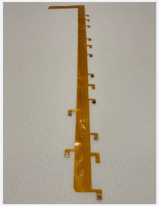 The automotive sector’s demand for revolutionary roofing glass aesthetics is one of the most adventurous challenges. And it is our engineering team’s innovation that is delivering sleek, capable, and robust electronic connector solutions to our Automotive Glazing clients for their PDLC Switchable Smart Glass Roofing designs.
| Section 9 |
Membership News |
||||
 Bill Wilkie Bill WilkieTechnical Director and Membership Secretary, ICT. |
New Members
ICT Register of Members
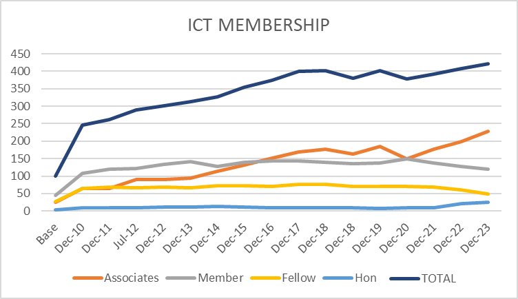
ICT Membership Grading 2010 - 2023 |
||||
| Go back to Contents |

ICT Council Members |
|
|
Council Members |
Emma Hudson (Chair), Andy Cobley (Past Chairman), Steve Payne (Hon Deputy Chairman), Chris Wall (Treasurer), William Wilkie (Technical Director, Hon Sec, Membership & Events), Richard Wood-Roe (Journal Editor & Web Site), Jim Francey, Martin Goosey, Lynn Houghton, Pete Starkey, Francesca Stern and Bob Willis, |
Editors NotesThe ICT Journal |
|
|
Richard Wood-Roe |
Instructions / Hints for Contributors 1. As it is a digital format the length is not an issue. Short is better than none at all! 2. Article can be a paper or a text version of a seminar or company presentation. Please include data tables, graphs, or powerpoint slides. We can shrink them down to about quarter of a page. Obviously not just bullet points to speak from. 3. Photo's are welcome. 4. We would not need source cross references 5. Title of presentation - Of course! Date, Job title of Author and Company represented. 6. An introductory summary of about 150 words would give the reader a flavour of what it's all about. 7. Style - we don't want out and out advertising but we do recognise that the author has a specialism in the product or process that will include some trade promotion. Sometimes it will be a unique process or equipment so trade specific must be allowed. 8. Date and any info relating to where or if this article may have been published before. 9. We can accept virtually any format. Word, Powerpoint, publisher, PDF or Open Office equivalents. 10. Also, to make it easy, the author can provide a word file to go along with his original powerpoint presentation and I/we can merge it together and select the required images. 11. A photo of author or collaborators. I really do look forward to receiving articles for publication. Richard Wood-Roe |