The Journal of the Institute of Circuit Technology Vol 12 No 1 November 2019 |
|
| Links to Contents | Section |
| Calendar of Events | 1 |
| 2 | |
| Council Members | 3 |
|
Obituaries: Stuart Cunningham, David Clayton, Bruce Routledge |
4 |
| 5 | |
|
ICT AGM and Evening Seminar at Leamington Spa - 26th Feb 2019 |
6 |
|
Annual Symposium and Fabricators Group Meeting at Black Country Musuem, Dudley - June 9th 2019 |
7 |
|
Autumn Evening Seminar at Meriden - 19th September 2019 with Presentation Video |
8 |
|
Preserving The Pest - Potential failure modes of tin lead -free alloys. |
9 |
| Annual Foundation Course - A History | 10 |
| 11 | |
| 12 | |
| Corporate Members | 13 |
| Publishers Notes | 14 |
| 15 | |
| Section 4 |
Membership News |
| 4.1 |
Obituary: Stuart Cunningham It is with sadness and regret that we announce the passing of Stuart Cunningham (68). Stuart was a popular figure on the ICT events circuit from 2005 – 2015, but had been ill for a number of years. Stuart started his working life (1966) as a mechanical engineering apprentice at Ferranti Edinburgh, where he spent much of his time in their captive pcb shop. He became a production engineer and then an industrial engineer at Ferranti before moving to procurement at GEC Marconi. Utilising his vast experience of pcb production, he joined Kam Circuits in 1992 as a tech sales engineer and then moved entirely to sales with what was then Cookson Electronics (Enthone) in 1995 as a product manager. The last ten years of his working life were spent at Kelan Circuits in Boroughbridge as product/technical sales manager. Stuart was hugely admired and adored by customers and colleagues alike. He would brighten a room with his many tales of Scotland and Ireland, along with his love of old bikes and rusty cars! He will be sadly missed. |
| 4.2 |
Obituary: David Clayton A full obituary will be published in the next issue. |
| 4.3 |
Obituary: Bruce Routledge Bruce Routledge Hon. Fellow - Long serving Member of the Institute - 1923 - 2019 Bruce was born in Dulwich in 1923, so he would have been 96 later this month. He studied Mechanical Engineering at the Twickenham Technical College, finishing his HNC the year after I was born. Most of his working life was spent in Uxbridge, where he started at the Bell Punch Company in 1944 as a Production Engineer and by the time it changed it’s name to Sumlock Anita Ltd (They developed the world’s first electronic desk calculator) in 1970, Bruce was immersed in Circuit Production in what was the early stages of the PCB Industry. In 1974, Bruce started CR Circuits with Doug Taylor (First ICT Chairman) and remained as Production Director till the company was sold to Graphic in 1989. Both were actively involved in the early stages of the Institute and for Bruce, this became a major life interest, utilising his layout and database knowledge as both Treasurer and Membership Secretary and latterly as Journal Editor. He joined as Associate Member on 5th June 1974, was made a full member 1986, a fellow in 1988 and appointed as Hon. Fellow by the council in 1997. A dedicated member of the Council, he attended meetings religiously until ill health took its toll, but he still kept in touch and having inspired the concept of the current journal was delighted to receive a clock as a memento of his eleven years as editor. He was an officer and a gentleman and we mourn his passing. http://www.anita-calculators.info/html/demise_of_anita_-_bell_punch.html |
| Go back to Contents |
| 4.4 | NEW MEMBERS |
|||
| Associate Members | ||||
|
Bill Wilkie: Technical Director and Membership Secretary |
10450 10451 10452 10453 10454 10455 10456 10457 10458 10459 10461 10462 10463 10464 10465 10466 10467 10468 10469 10470 10471 10472 10473 10474 10475 |
Jerry Richards Dee Downton Lukasz Jacko 10453 Dan Hudson 10454 Peter Blincow 10455 Robert Jordan 10456 Tom Foy 10457 Paul Duke 10458 Matthias Rupp 10459 Ian Pritchard 10461 Diana Scodreanu 10462 Lee Shelley 10463 Jason Takle 10464 Khloe Rowsell 10465 Chris Sharp 10466 Andy Grieve 10467 Callum Warnock 10468 Radoslaw Szczerbinski 10469 Martin Wolf 10470 Craig Stead 10471 Craig Hellon 10472 Roland Ebert 10473 John Rowley 10474 Liam Seddon 10475 Emily Copeland |
Leonardo GSPK GSPK GSPK HMGCC HMGCC HMGCC HMGCC Ventec-Europe Amphenol-Invotec Amphenol-Invotec Electra Eurotech Group Eurotech Group Eurotech Group Eurotech Group Zot Engineering Zot Engineering Merlin Flex Merlin Flex Merlin PCB Group RUAG Newbury Electronics CCE Europe CCE Europe |
|
| Members | ||||
| 10476 | Mike Hill | Express Circuits | ||
| Re Instatement | ||||
| 9700 | Gary Gibbens | Atotech | ||
| Go back to Contents | ||||
| Section 6 |
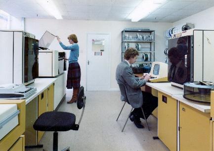
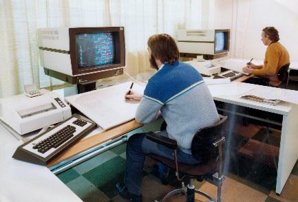
Institute of Circuit Technology Evening SeminarWoodland Grange Hotel, Leamington SpaTuesday, 26th February 2019 |
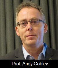 |
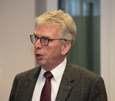
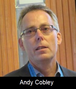
As the sun set on a glorious February day, which could easily have been moved from Spring to give us foretaste that better weather was on its way, the Institute of Circuit Technology hosted its first 2019 seminar at the Woodland Grange Hotel in Royal Leamington Spa in the Midlands of England. The diverse programme of four presentations was introduced by ICT Chairman, Professor Andy Cobley, of Coventry University, who stood in for Bill Wilkie, who had been taken ill at short notice. Andy thanked Bill for his hard work in organising the seminar. He also noted that Pete Starkey was recovering from a recent accident and wished him a speedy recovery. |
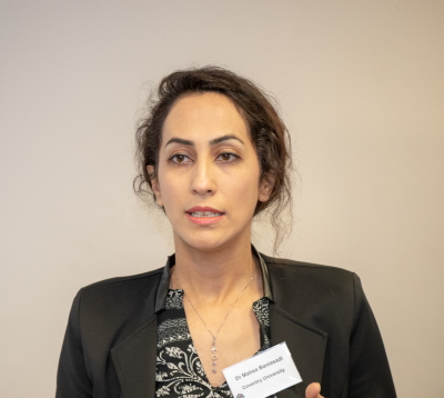 |
The first presentation was on ‘Bioleaching of Metals from PCBs’, and was given by Dr Mahsa Baniasadi of Coventry University. The project had been supported by Innovate UK and had an industrial partner. The potential for metal recovery from electronic waste (WEEE) was highlighted, given that there were around 44.7 metric tonnes of WEEE produced annually around the world. A comparison of the metal contents of PCBs and ores was shown, to highlight the potential for recovering metals from such waste. The conventionally used pyro- and hydro-metallurgical recovery methods were described, but more sustainable approaches were needed. Bioleaching was one such method and relied on the production of acids and ligands via the use of micro-organisms. The mechanisms employed were detailed; for example, biocyanidisation could be used for gold recovery, using cyanogenic bacteria to produce the requisite cyanide. The microorganisms could also be used to subsequently degrade the cyanide. The chemical reaction of the metal cyanide complex formation reaction was shown and comparisons had been made between biocyanidation and chemical cyanidation approaches. The bio process had a lower cost and a life cycle assessment had been undertaken. ‘Non-metal content’ removal was an important prerequisite for metal recovery and this was described; it could include the use of a shaking table and electrostatic separation. Data for base metal recovery was also presented and the effect of operational parameters was reviewed. Key factors impacting the recovery efficiency included the glycine concentration, pH, pulp-density, dissolved oxygen levels and particle size. Finally, a commercial metal extraction approach known as the ‘Merrill Crowe’ process was described and this used activated carbon, ion exchange and electrowinning. |
 |
The second presentation was on ‘Soluboard – a New Composite for Electronics’ and this was given by Jonathan Swanston of Jiva Materials. The Jiva company was only just over a year old and its aim was to redefine the way printed circuits were made, with particular emphasis on a fully recyclable PCB laminate that could replace FR4. The problems with end-of-life PCBs, and their traditional methods of treatment, were detailed. These included the release of toxins into the environment. The new product was called Soluboard and it was based on the use of a natural fibre reinforced composite and a soluble polymer which dissolved in hot water. The product was flame retarded using phosphorus based material, fully biodegradable and non-toxic. The potential market for the product in the context of the overall substrate market was described and the current focus was supplying to EU instrumentation makers, where there was said to be a lot of interest. The current price was around £20.00 per square metre and the aim was also to supply it to domestic appliance manufacturers. The company was currently working with Printed Electronics Limited (PEL) and Loughborough University and proof of concept had been demonstrated. The key properties were favourably compared to those of FR4. |
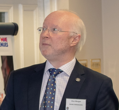 |
The third presentation was called ‘Developing universal solutions to automotive materials challenges’ and was given by Alun Morgan of Ventec. Alun had very kindly stepped in at the last minute to replace the scheduled speaker, Emma Hudson, who had unexpectedly been called away on a business trip. Alun began by outlining the automotive application hot spots requiring thermal management and described LED lighting and its advantages, such as lower power consumption and long lifetime. Haitz’s law was outlined and it described how the cost per lumen fell by a factor of 10 per decade and, for a given wavelength, the amount of light generated per package increased by a factor of 20. He then introduced the basic thermodynamics and outlined the principles of the first, second, third and “zeroth” laws. The principles of the transfer of heat were also described and convection, conduction and radiation were detailed in the context of LED thermal management. LEDs were more efficient than incandescent lamps, but almost 75% of the input electrical power was turned to heat. The conventional methods of managing the heat from LEDs included the use of heatsinks but there were other important methods including the use of thermally conductive PCBs that had enhanced thermal properties compared to FR4. The thermal conductivities of a range of well known materials were listed, and the equations relating to convective and radiative heat transfer were shown, along with an example calculation model for thermal radiation. The critical importance of being able to survive thermal cycling, e.g. in a headlamp unit, was illustrated through the use of two case studies where failure had occurred. Failure analysis had shown that the CTE mismatch between various materials used in the construction had been the likely cause. The problem had been resolved by using materials with more closely matched CTEs and by optimising moduli. The future requirements were illustrated by reference to the published industry roadmaps. |
 |
The final presentation of the evening, entitled ‘Back to Basics’, was given by Ian Mayoh of Ventec, who began by giving a description of PCB base materials and detailing the various types of resins systems and why they were used. He then discussed the range of glasses and other reinforcements: for example, D glass and NE glass both found use in low loss/high speed applications. He used a schematic to show the production process stages for base materials. The brominated flame retardants and alternative organo-phosphorus materials were described and their functional mechanisms were explained. In recent years, there had been a move away from the use of dicyandiamide curing agents to the phenolic-based systems, which were needed to provide compatibility with the higher temperatures encountered with lead-free soldering. He presented data showing the differences in laminate thermal expansion below and above the glass transition temperature (Tg) and explained techniques for measuring Tg such as differential scanning calorimetry (DSC) and thermo-mechanical analysis (TMA). He discussed the dielectric properties of the various materials used in making a laminate and reviewed the effects of dielectric constant on board design and signal integrity. Copper foil profile was another increasingly important consideration, particularly for boards working at higher frequencies where the skin effect meant conduction was only in the outer few microns of the copper. Again, the presentation concluded with reference to future substrate trends as recorded in the latest industry roadmaps. |
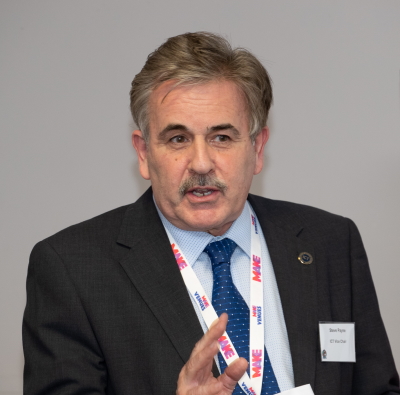 |
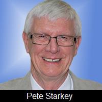
The meeting was closed by Steve Payne, who invited members of the ICT to participate more by considering submitting papers to the ICT journal or by joining the ICT Council. He asked the audience to thank the four speakers for their excellent presentations. Finally, Steve asked the attendees to offer their thanks to Ventec International for the kind sponsorship of the seminar, and the response was a loud round of applause. Martin Goosey 26th February 2019 Footnote: I most gratefully acknowledge the efforts of Professor Martin Goosey in preparing this review, and of Alun Morgan for providing the photographs. Many thanks! Pete Starkey. |
| Go back to Contents |
| Section 7 |
Annual Symposium and Fabricators Group Meeting Black Country Musuem, Dudley - June 9th 2019 |
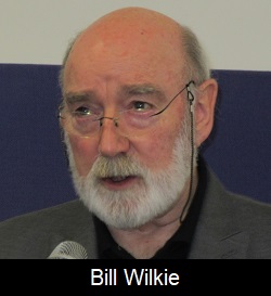 |
“Yam awlroight, aer kid?” A friendly greeting in the local dialect as the Institute of Circuit Technology (ICT) held its 45th annual symposium June 4, 2019 in Dudley at the Black Country Museum—a symbol of the spirit of innovation in engineering technology and the entrepreneurial and manufacturing skills that had established that region’s supremacy in leading the original Industrial Revolution. ICT Technical Director Bill Wilkie opened the proceedings with a good-humoured welcome address in which he likened delegates to kernels of knowledge and the ICT to a metaphorical watering can that encouraged their knowledge to germinate, flourish, blossom, and propagate. |
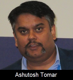 |
He was delighted to introduce keynote speaker Ashutosh Tomar, technical manager (research) with Jaguar Land Rover—the U.K.'s largest automobile manufacturer. Tomar’s speciality was the development of smart surfaces, structural and flexible electronics. His presentation entitled "Applications of Flexible and Hybrid Electronics in the Car" gave delegates the opportunity for a privileged look at some of the advanced electrical and electronic features hidden beneath the bodywork and interior trim of Jaguar Land Rover vehicles. "Today’s automotive industry is as high-tech as aerospace. The electrical architecture is growing exponentially," said Tomar. He continued, "In our premium vehicles today, we have at least 175 features—probably double that if we include connected-car features and infotainment. The rate is continuing to increase with advances in self-learning, electric, and autonomous vehicles, which directly impact what goes underneath the body. And we have an ever-growing number of electronic control units in the car together with a rapidly increasing volume of sensors and smart sensors and their associated input-outputs and actuators inside of the car. There’s no room to put any more electronics!" To illustrate some realities, Tomar’s graphics showed the locations of over 100 sensors, the enormity of a traditional wiring harness—eight kilometres of wire weighing 90 kilograms—and the complex labour-intensiveness of its construction. Tomar saw flexible circuits as the future of electrical distribution systems, and structural electronics as enablers for lightweight electronics features—such as displays, interior lighting, haptic sensing, and gesture recognition systems—building them into visible hard and soft surfaces within the car interior. He passed around an example of an integrated overhead lighting and control panel made by injection-moulded structural electronics technology, which offered a thickness reduction from 50 mm to 3.5 mm—a 60% weight saving and a 70% reduction in physical bill of materials. Tomar went on to discuss possibilities in self-sustained wireless sensors—containing sensing, energy harvesting, battery technology, and transmission all in one package—and adapting flexible circuit and printed electronics capabilities to integrate electronic control units and electrical distribution systems. The effect would be to dramatically reduce mass and volume to eliminate large numbers of connections and achieve logistic benefits and a high level of automation in manufacture. Although there remained some technical challenges to overcome and many thousands of hours of reliability testing to complete, it was only a matter of time before the full benefits of these concepts would be realised. It was clear that form was becoming at least as important of a consideration as a function: “What we can do is only limited by our imagination and vision!” Tomar’s keynote certainly captured the imagination of his audience and provided the basis of a very lively question-and-answer session. |
 |
The closely related topic of printed electronics technology was the subject of the presentation by Jack McGhee who had recently completed a post-graduate study of new materials and methods at Loughborough University. Loughborough has a long history of formulation and characterisation of materials for printed electronics. McGhee explained that although the printing of conductive materials enabled inexpensive mass production of electronic devices that could be thin and flexible, those devices would typically have lower performance than conventional electronics. Whereas silver and carbon inks had most commonly been used, his research had examined the effects of integrating ceramic conducting and semiconducting materials into inks to improve their properties and increase their functionality. He discussed the incorporation of metal oxides, such as gallium-zinc oxide and indium-tin oxide, and more complex oxides, such as ferrites. As printed, these materials gave some advantages over straightforward silver and carbon, but to achieve optimal conductivity, the materials required sintering and fusing. Of the several post-processing techniques investigated, some interesting results had been achieved with laser scanning, which could give effective local temperatures between 800°C and 1,300°C and decrease resistivities from typically 50 ohms per square to 3 ohms per square. Whereas originally it had been believed that simple fusing was the primary effect, McGhee demonstrated how the nanostructure of the materials could be manipulated by altering parameters and explored possible mechanisms. With indium-tin oxide, there was evidence that crystal growth occurred during re-oxidation, such that it formed microscopic wires and branched structures. And that the final structure depended on laser power and the optical properties of the material. He showed several examples. Applications for laser-treated printed metal oxides included frequency selected surfaces, high-surface-area coatings for sensors, printed films for solar cells, tuneable capacitors, printed humidity sensors, and printed temperature sensors. There were also potential applications in 3D printed sensors. Ongoing printed electronics projects at Loughborough included screen-printed textile supercapacitors, printable active devices, and power dissipation through printed materials. |
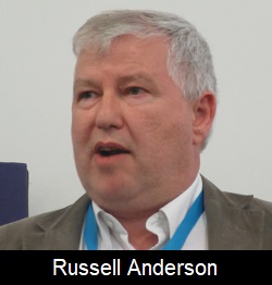 |
Extending the printed electronics theme to include stretchables, the final presentation of the morning session came from Russell Anderson, senior technical support specialist with DuPont Photovoltaic & Advanced Materials. “We know textiles, and we know electronics,” was a justifiable claim of DuPont with many years of history in those individual areas of expertise. And more recently, they had the opportunity to combine the two in wearable applications, for which a huge market was forecast and stretchability was a desirable attribute. Anderson explained some of the science of wearable and stretchable performance, which required a balance between comfort and function, with reference to graphs of mechanical stress and electrical resistance versus strain. He also described a stretchable bi-layer thermoplastic polyurethane film composed of high-recovery and melt-adhesive layers supplied on a temperature-stable carrier. It was also designed so that a stretchable ink could be printed on the high-recovery surface and the melt-adhesive layer used to hot-press bond it to the fabric. A silver-loaded screen-printing ink had been developed with the metal in the form of fine flakes suspended in a thermoplastic elastomer resin. During the drying step, the solvent was removed, and the conductive particles packed together forming electrical pathways. He showed the results of 100% stretch testing and 80-cycle 10% strain testing—both of which maintained low electrical resistance—and functional wash testing based on 50 cycles of the ISO 6330 colour fastness test with minimal increase in resistance. A typical volume production sequence for the incorporation of conductors into apparel was to screen-print circuits onto the polyurethane substrate, singulate the patterns by die-cutting or laser-cutting, hot-press-bond the circuits onto fabric, add any functional components, and then assemble the garments. Applications included sportswear for monitoring respiration and heart rate, heated industrial winter wear, and various medical monitoring functions and automotive heaters and sensors. |
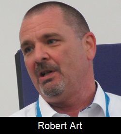 |
Dodging the showers, delegates made their way down the hill to the authentic reconstruction of a 1930s High Street and queued up to enjoy a traditional lunch at Hobbs and Sons Fish and Chip Shop. Some paused to admire the Sunbeams at Hartill’s motorcycle shop and had to hurry back uphill to return to the conference room and the 21st century for the afternoon session. "High performance automotive and power electronics begin with innovative materials," was the opening line of an enlightening discussion of insulated metal substrates and thermal interface materials from Robert Art, global account manager IMS/TIM for Ventec International Group. He listed the basic components of a typical IMS material—a metal base layer, a dielectric layer, and a circuit layer. Then, he looked more deeply into the realities of their properties and how they needed to be considered from a different perspective than those normally associated with FR-4 laminates when specifying materials for particular applications. Beginning with glass transition temperature (Tg), for the gradual and reversible transition in amorphous materials from a hard and relatively brittle state into a rubbery state with increasing temperature, the popular perception was that this should be very high. This was true for achieving mechanical stability in regular FR-4 multilayers, but in IMS materials, a lower Tg was preferable. This enables the dielectric to act as a compliant interlayer between components with expansion coefficient typically 10 ppm/°C and the aluminium baseplate with expansion coefficient typically 23 ppm/°C, hence reducing any tendency to cracking of solder joints under thermal cycling. Clearly, the primary reason for using IMS substrates was to conduct heat away—“LEDs get destroyed not because of current but because of heat”—but there was still some confusion in terminology (e.g., thermal resistance, thermal impedance, thermal conductivity, etc.) and different test methods could give widely different results. It was important that the customer carried out their own tests before specifying a particular material rather than relying on nominal data-sheet values. Voltage-withstand testing depended on the application and was linked to the operating voltage of the system. UL required the test voltage to be twice the operating voltage plus 1,000, and users typically asked for higher values than that. Art emphasised that each test stressed the material, and the circuit should still work after testing rather than be tested to destruction. He went on to discuss Ventec’s range of IMS materials, and the technology roadmap showing the typical applications for which they had been developed. In applications where solder-joint cracking was a critical reliability issue, the newer materials had dielectrics designed for elastic deformation and low-expansion aluminium alloys to minimise mechanical stressing. Art examined a series of alternative design concepts for thermal management with IMS substrates and special surface treatments and demonstrated applications and benefits of electrically conductive and insulating thermal interface materials. He emphasised the importance of choosing the right material from a cost-performance standpoint but added a note of caution in advising OEM designers to avoid nominating too many different materials and causing inventory and stock-control problems for the PCB fabricator. |
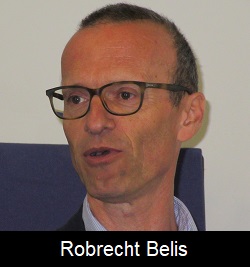 |
Taking the guesswork out of copper distribution in pattern plating operations was the subject of the final presentation by Robrecht Belis, manager of the Surface Finishing Business Unit at Elsyca in Belgium. Achieving relatively uniform deposit thicknesses across complicated panel designs was a task that had historically relied heavily on the combined experience of pre-production and process engineers and had inevitably involved a lot of trial-and-error and compromise. Belis described graphical simulation software that could be straightforwardly configured to a specific plating geometry and electrolyte, panel size and pattern, and process parameters based on a virtual mockup of the real-life plating tank and flight bar. Alternative panel configurations and the effects of shields and robbers could be quickly evaluated. The software enabled a substantial improvement in plating uniformity and provided detailed information on copper thickness distribution and potential quality issues. |
 |
ICT deputy chairman Steve Payne, managing director of Cirflex Technology Ltd, brought the symposium to a close, thanking speakers for sharing their knowledge and the quality of their presentations, delegates for their attention and support, and particularly Bill Wilkie for organising an exceptionally interesting and relevant programme |
| Go back to Contents |
| Section 8 |
Autumn Evening Seminar at MeridenSeptember 19th 2019 |
 |
An ancient monument dating back more than 500 years stands proudly on the green in the village of Meriden with a plaque stating that, by tradition, it marks the centre of England. But more recently, GPS technology argues that the true geographical centre is 11 miles north! Either way, Meriden has been established as a popular Midlands venue for Institute of Circuit Technology (ICT) meetings. On September 19, a multitude of Fellows, Members, and Associates gathered for the Institute’s autumn seminar, which was organised and hosted by ICT Technical Director Bill Wilkie. The agenda included five informative technical presentations, describing current research and development on significant topics relevant to the industry. |
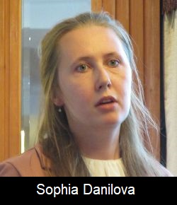 |
Sophia Danilova, a Ph.D. student worker from the Research Centre for Manufacturing and Materials Engineering at Coventry University, discussed the importance of selective metallisation in the electronics sector. Her presentation titled entitled “Selective Electroless Copper Plating on a Non-Conductive Substrate Via Magnetic Field Application” included a discussion of PCBs, moulded interconnect devices, microelectronics, printed electronics, wearable technology, and radio-frequency identification devices. It had been estimated that 30–40% of the total manufacturing cost of an electronic device was due to photolithography, a time-consuming, multi-step process with high material wastage due to coating the entire surface with photoresist before exposure and development to create a resist pattern. Patterning by magnetic field was being investigated as a lower-cost alternative with shorter processing time. The objective was to selectively deposit a catalyst and then to build the conductor pattern by electroless copper deposition. The first step was to prepare a suitable magnetic catalyst. Initial attempts to combine silver and iron powders by ball-milling resulted in particle sizes that were too large for accurate patterning. Iron-palladium nano-particles supplied by the specialists at the Jožef Stefan Institute in Slovenia were found to be unsuitable for the application. Wet chemical synthesis of a composite of silver and iron oxide using arginine as reducing agent gave promising results, and wet chemical synthesis of a composite of silver with silica and iron oxide using tin as a reducing agent gave particles with a regular distribution of magnetic and catalytic sites. The conditions for magnetic deposition of a catalyst had been optimised in terms of time and pH as determined by the uniformity of electroless copper coverage. Magnetic templates were designed using finite element method magnetics (FEMM) software for the simulation of magnetic field distribution. Copper patterns with micron-scale features had been successfully produced by electroless plating, and the research had progressed from idea to proof of concept. The main goal of future work was to selectively deposit copper in sub-micron patterns by creating mono-dispersed magnetic nanoparticles, continuing work on template modelling using 3D simulation software and the optimisation of catalyst and copper plating conditions. |
 |
Professor and ICT Chairman Andy Cobley from Coventry University gave a two-part presentation, including an update on the MATUROLIFE project in which the university was a partner and an introduction to the ReCollect project in which the Institute was a partner. The Horizon 2020 funded MATUROLIFE project was in its 20th month out of 36, and Cobley reported its progress in the areas of design, materials, electronics integration, and prototype manufacturing. The consortium of 20 partners from nine European countries brought a creative and artistic design together with materials science and electronic manufacturing to produce innovative assistive technology co-created with older adults across Europe to support independent ageing and well-being. Fundamental to the concept of smart textiles was a practical metallisation process, and extensive work had been carried out to compare different catalysts for the electroless copper plating of polyester, nylon, and cotton fibres. A copper-nanoparticle formulation had given better results than standard colloidal palladium, based on the conductivity of the electroless deposit. By adding polyethylene glycol to adjust viscosity, an inkjet-printable version of this formulation had been produced which had been used to produce high-resolution images on fine polyester fabric. Various organic post-treatments were evaluated for the protection of conductive tracks against perspiration and repeated washing. Cobley also showed examples of the integration of electronics by embedding smart textiles into a range of clothing, furniture, and footwear solutions. Concept prototypes had been manufactured, and opportunities for industrial scalability were explored. And in the second part of his presentation, Cobley introduced the ReCollect project funded by Innovate U.K., in which ICT had undertaken to support the stimulation and dissemination of U.K. industry feedback on the developments. It had been estimated that the annual world demand for FR-4 glass-epoxy circuit boards was approaching 20 billion square metres, of which about 15% was single- and double-sided. It was not practical to salvage the fibreglass and epoxy-resin components at end of life. Generally, recycling was limited to shredding and incinerating to recover precious metals. The ReCollect project proposed an alternative route to managing end-of-life circuit boards by removing glass-epoxy materials from the supply chain and establishing an efficient manufacturing process for non-toxic, recyclable, composite laminates. One of the project partners had already demonstrated the feasibility of reinforcing water-soluble materials with natural fibres to use as substrates for single- and double-sided PCBs. The primary aim of the project was to demonstrate the feasibility of producing this material in high volumes within the U.K. and show that it could match the performance of CEM 1 and FR-4. The secondary aim was to investigate means of chemically protecting the material from existing aqueous processes used in PCB manufacturing. Another of the project partners was developing a novel process for the continuous production of sheet material. The overall market opportunity was substantial, although there would inevitably be a need to overcome the expected inertia in transitioning from a long-standing existing technology. |
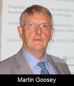 |
Recognised for many years in the printed circuit industry for his outstanding contribution to science and technology—both academically and practically—as well as for his environmental awareness and commitment, Professor Martin Goosey drew delegates’ attention to the finite supply of key raw materials to the electronics industry. Particularly, he emphasised the scarcity of platinum-group metals (PGMs), the growing global demand, and the importance of recovering and recycling these materials to bridge the increasing gap between supply and demand. Goosey had a long-standing interest in recovering materials from PCBs and waste electrical and electronic equipment (WEEE). Indeed, I remember him chairing the Environmental Working Group of the Printed Circuit Interconnection Federation, studying opportunities for PCB recycling over twenty years ago. More recently, changes in technology have been driving the demand for critical raw materials. Examples include the move from CRT towards LCD and OLED displays, the replacement of incandescent lighting with LED, the evolution of battery technology from nickel-cadmium through nickel-metal-hydride to lithium-ion, and the transition of vehicle propulsion systems from the internal combustion engine to battery power. Europe had been estimated to have the highest annual demand of PGMs in the world—40 tonnes, worth over 1100 million Euros—and globally, there was currently an annual shortfall of about 20 tonnes between demand and what could be supplied from primary sources. And the shortfall was forecast to continue to grow. End-of-life recycling became even more relevant, especially considering that the concentration of PGMs could be at least 100 times greater in electronics wastes than in natural ores. The traditional method was to shred the waste and burn it; there was an urgent need to develop viable methods for recovering valuable materials at end of life. Further, Goosey gave an introduction to the PLATIRUS Project—Recovery of Critical Raw Materials from WEEE—funded by the European Commission as part of the Horizon 2020 Research and Innovation programme. His company, Env-Aqua Solutions Ltd., was one of 12 partners representing industry, research, and academic organisations across the value chain. The objective of the PLATIRUS Project was to help bridge the supply-demand gap of PGMs in Europe by developing and introducing novel secondary raw materials to the recovery supply chains of automotive catalysts, mining, and electronic wastes. The project aimed to develop a miniaturised recovery process for platinum-group metals based on selection and optimisation of a cost-effective combination of advanced hydro-metallurgy, iono-metallurgy, supercritical CO2 extraction, solvo-metallurgy, pyro-metallurgy, hydro-metallurgy, and electro-winning technologies, and to upscale the process to industrially relevant levels. Apart from the obvious advantages of bridging the supply-demand gap and reducing Europe’s dependence on global PGM supply chains, the PLATIRUS Project offered potential benefits in reducing energy costs and environmental impacts as well as providing solutions requiring lower capital investment than centralised refineries and maximising the exploitation of local waste sources. The work of the PLATIRUS Project was due to be completed and the final report published in October 2020. |
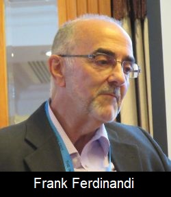 |
Frank Ferdinandi, director of Azurion Technology described an environmentally friendly surface finish for PCBs, which was effectively an ultra-thin fluorochemical conformal nano-coating deposited and polymerised in-situ by a plasma process. Where the coating was deposited on copper, it offered long-term protection against oxidation, but the copper remained solderable by standard techniques. Elsewhere on the PCB, it provided a durable waterproof finish. Ferdinandi showed samples of boards coated more than 10 years previously, using an early version of the finish. The copper remained bright and tarnish-free, but still easily solderable. There had been a programme of continuous development, and the current finish represented the third iteration. Ferdinandi explained that the new technology outperformed existing surface finishes in key areas and provided major advantages for PCB protection and post-processing. Its functional benefits included excellent long-term protection against oxidation together with a solder-through capability compatible with current reflow processes for lead-free and leaded solders. After soldering, its non-wetting properties across the complete surface gave circuits increased resistance to aggressive environments, resulting in longer product life with no rework issues. A major environmental benefit was that since no water was used, the effluent associated with traditional surface coating processes was eliminated and health and safety issues were significantly reduced. Plasma deposition was carried out in a single chamber, and in-situ cleaning was possible. The system could be semi-automated for high throughput. Solderability, solder joint reliability, and electrical properties had been extensively studied and compared favourably with immersion silver, HASL, OSP, ENIG, electroplated nickel-gold, and immersion tin. Although previous commercialisation programmes had shown only limited success, there was currently renewed interest—particularly from China—where the opportunity to reduce water consumption was especially attractive. Frank has kindly provided a video of his slide presentation which can be viewed from this link |
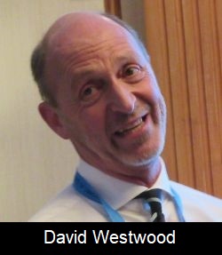 |
The team behind Rainbow Technology Systems introduced a specialised surface-cleaning technology to the printed circuit manufacturing industry over 30 years ago. Their system of contact sheet-cleaning and web-cleaning solutions, based on rubber pick-up rollers lifting minute particles from surfaces and transferring them to an adhesive roll, became the industry standard. David Westwood, Rainbow’s sales and marketing manager, explained how this proven technology maintained its relevance and impact in the advancement and development of ultra-fine-line circuitry. Aided by a series of animations, and frequently wielding a small hand-held pick-up roller and a pad of adhesive sheets for dramatic effect, Westwood demonstrated the potential effect of dust-related imaging defects on manufacturing yield. His illustration of typical dust and debris on a design of the 1980s with 300-micron track and gap included particles varying in size, including 75–100 microns, 50 microns, 25–30 microns, and down to 15 microns. At this level of design rule, even if the efficiency of cleaning was only 98%, any issues associated with the remaining 2% could be touched in by a skilled operator with a steady hand. It’s not so for current designs with track and gap trending towards 15–20 microns! The KSM Superclean division of Rainbow Technology Systems had stayed ahead of the technology and was confident that contact cleaning remained the most effective method of removing debris from surfaces. Roller and adhesive technologies had been developed that enabled greater efficiency of cleaning to 99.9% at finer particle sizes down to the 0.5–3-micron critical levels. Harder rollers were available with precision surface finishes, silicone-free, and static-dissipating. And the adhesive rolls were based on clean-room film materials. Westwood believed that contact cleaning would continue to be the most effective means for the permanent removal of surface debris as design technology progressed from fine-line to ultra-fine line. |
| Cobley brought the seminar proceedings to a close, thanking the audience for their attention and the presenters for generously sharing their knowledge. A special thanks went to Bill Wilkie for another superbly organised learning and networking event. | |
| Go back to Contents |
| Section 9 |
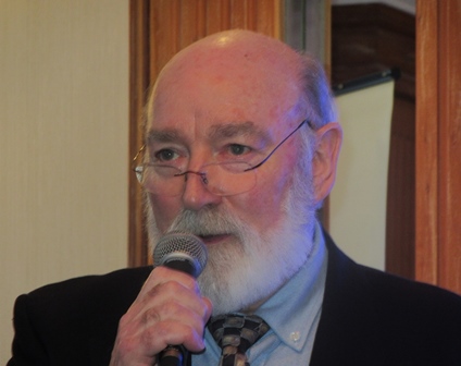
Preserving The Pest!Bill Plumbridge,Emeritus Professor of Materials EngineeringThe Open University |
|
Bill Plumbridge |
The emergence of lead-free alloys just over a decade ago brought with it two major challenges. Traditional tin-37 mass percent lead had a low melting point (183oC) whereas the new generation, based primarily upon tin with a few percent of elements such as copper, silver, zinc or bismuth, melted around 220oC. This caused problems in the manufacturing stage of electronic goods although these have largely been overcome. A second problem which is much more long term relates to the performance of soldered joints in electronics equipment. Because the new alloys are predominantly tin, they are likely to be susceptible to the peculiarities of that element. Tin is allotropic and one of its transition temperatures occurs in the middle of many likely service conditions. Above 13.2oC, it has a body centred tetragonal crystal structure (white tin) while below this temperature, diamond cubic structure (grey tin) predominates. Even more significant is the 27 percent volume change associated with it, which could have profound effects on the integrity of soldered joints made from such alloys. The transition is associated with the formation of surface eruptions, or warts, known as tin pest. The process occurs by nucleation and growth, with the time for the former varying from several months to many years according to the temperature.(1) Unlike most metallurgical reactions of interest which can be accelerated by increasing temperature, the thermodynamic driving force for tin pest formation is achieved by lowering the temperature but concomitantly the kinetics are slowed. This means that a study of tin pest formation and growth requires great patience! In a major programme on the mechanical behaviour of the, then, new lead-free solder alloys, The Solder Research Group at the Open University discovered tin pest on many of their samples stored and tested below 0oC. A spin off programme focussed upon tin pest itself yielded numerous publications (2, 3) and some extremely valuable, from the scientific standpoint, samples. BUT the end is nigh! Most participants have dispersed; only a fraction of the original samples remain, and these are now under threat. Because of the impossibility of natural ageing these samples are extremely valuable scientifically. If, heaven forbid, joint failure due to tin pest begins to occur, their worth technologically will be immeasurable. These samples are available to any interested party willing to continue the study. To date, microstructural examination has been limited, so there is plenty of scope for PhD research. Above all, this represents an opportunity to close the door before the horse has bolted. For further information, please contact me. Bill Plumbridge, Emeritus Professor of Materials Engineering The Open University
References
Figure Caption Total disintegration of a tin-0.5 copper sample after prolonged exposure at – 180C |
| Go back to Contents |

| Section 12 |
Industry News |
| 12.1 |
Adeon Technologies is pleased and proud to announce her new cooperation with ESI Inc. from Portland OR, USA for the representation of the ESI Laser Drilling & Routing Portfolio in the European Printed Circuit Board manufacturing industry. During construc
tive meetings between the companies it rapidly became apparent that ESI and Adeon realised this partnership makes perfect sense to join forces for the European PCB industry. |
| 12.2 |
The next revolution in electroless copper for advanced FPCB |
| 12.3 |
At last, some news regarding Parliament that doesn’t involve brexit! CC Electronics is proud to have taken part in a Parliamentary Review, focusing on manufacturing and services. It profiles small and medium enterprises, who have been identified as successful in their field. Click on the link here parliamentary-review to read the full detail. |
| 12.4 |
The Eurotech Group are on track with their fire recovery program. "We have taken delivery of our new Direct Metallisation and Layer Preparation lines, which are being installed and tested during May. In the meantime our new Develop Etch Strip & Chemical Clean lines have been signed off by our technical team and are in the process of being shipped." The new Photomech cleanroom has been completed and is currently being fitted out ready to be brought into use during May. Our new Plating Line and main Multilayer Press facilities are to be delivered and installed during June and July. Read more... |
| 12.5 |
Exception PCB have been awarded PCB Manufacturer of the year 2019 by Industrial Process News. Industrial Process News is an independent publication that circulates 5,000 printed copies on a national basis to decision-makers involved in the UK’s industrial and process markets. We have been making significant improvement since a new management team took over the business in 2017. Read more... |
| 12.6 |
Merlin PCB Group have released a short video of how a pcb is manufactured . This was filmed at the Merlin PCB Group “Rigid” manufacturing plant at Deeside in North Wales. Read more... |
| 12.7 |
UK First for GSPK GSPK Circuits are thrilled to announce that they are the first PCB Manufacturer in the UK to install a new line to produce the exciting new EPAG finish. EPAG Electroless Palladium Autocatalytic Gold is a new direct palladium surface finish process with an optional gold layer. Atotech has developed the advanced PallaBond process, which allows […] |
| 12.8 |
Amphenol Invotec wins Rolls Royce Supplier of the Year award Electronics and printed circuit boards manufacturer, Amphenol Invotec has been honoured at the 2019 Rolls Royce Supplier Conference with the highly coveted ‘Supplier of the Year’ award. The conference took place on 18 July in front of an invited audience of 50 top suppliers to Rolls Royce from all over the world. Read more..... |
| 12.9 |
We are HMGCC, Her Majesty's Government Communications Centre. We design and deliver communication systems and provide technical solutions that protect national security at home and overseas, now and for the future. Ours is a world of pioneering products, custom one-offs and very special builds - where ideas and ingenuity are helping protect the UK and its interests in this ever-evolving digital age. Our teams create high-tech products featuring design and engineering of incredible complexity. But while our products can be tiny in size, their importance to the security of the country is immense. Read more... |
| 12.10 | Holders Technology UK is located on the outskirts of Galashiels in the Scottish Borders. It was established in 1987 and offers a range of specialist materials as well as consumables to the UK PCB industry. Holders Technology UK is part of the Holders Technology Group, which is listed on the AIM market of the London Stock Exchange. For further information please visit ww2.holderstechnology.com |
| 12.11 |
Minitron Managing Director - Paul Goodfellow has kindly supplied the editorial for this issue. Read more... |
| 12.12 | Stevenage Circuits gain Cyber Essentials PLUS Accreditation. Cyber Essentials PLUS has exactly the same requirements of Cyber Essentials, however, the critical difference is that Cyber Essentials PLUS requires an independent assessment of SCL's security controls. As a result, Cyber Essentials PLUS has become a much more highly regarded certification. Read more... |
| 12.13 |
Ventec are pleased to announce the addition of two new thermally conductive thin isolation foil materials to our range of Thermal Interface Materials (TIM) under our distribution agreement with EMI Thermal. Initially for the European market, Ventec teamed up with EMI Thermal to provide a range of Thermal Interface Materials (TIM) that are a perfect complement to Ventec’s IMS material families, thermally conductive and standard laminates and prepregs for multilayer PCB’s. The range of materials distributed through Ventec, which includes double sided thermal tape, electrical insulators, natural graphite and void fillers, has now been expanded with the addition of two new UL94 V-0-recognized thin isolation/thermal conductive foil materials. Read more... |
| 12.14 | Zot is happy to announce that they have placed an order for a new Cupric Etch and Resist Strip Line from UCE - supplied and installed by Viking Services UK Ltd. The new process line increases capability and capacity for processing high technology, high reliability Printed Circuits. Read more... |
| Go back to Contents |
|
Corporate Members of The Institute of Circuit Technology September 2018 |
||
| Adeon Technologies BV |
Weidehek 26,A1 4824 AS Breda,The Netherlands |
www.adeon.nl |
| Atotech UK Ltd. | William Street, West Bromwich. B70 0BE | www.atotech.com |
| CCE Europe | Wharton Ind. Est., Nat Lane, Winsford, CW7 3BS | www.ccee.co.uk |
| ECS Circuits Ltd. | Unit B7, Centrepoint Business Park, Oak Road, Dublin 12, Ireland | www.ecscircuits.com |
| Electra Polymers Ltd. | Roughway Mill, Dunks Green, Tonbridge, TN11 9SG | www.electrapolymers.com |
| The Eurotech Group | Salterton Industrial Estate, Salterton Road, Exmouth EX8 4RZ | www.eurotech-group.co.uk |
| Exception PCB Solutions | Ashchurch Business Centre, Alexandra Way, Tewkesbury, Gloucestershire. GL20 8NB | www.exceptionpcb.com/ |
| Merlin PCB Group | Hawarden Industrial Park, Manor Ln, Deeside, Flintshire, North Wales, CH5 3QZ | www.merlinpcbgroup.com |
| Faraday Printed Circuits Ltd | 15-19 Faraday Close, Pattinson North Ind. Est., Washington. NE38 8QJ | www.faraday-circuits.co.uk |
| Graphic plc | Down End, Lords Meadow Ind. Est.,Crediton EX17 1HN | www.graphic.plc.uk |
| GSPK (TCL Group) | Knaresborough Technology Park, Manse Lane, Knaresborough HG5 8LF | www.gspkcircuits.ltd.uk |
| Invotec Group Ltd | Hedging Lane, Dosthill, Tamworth B77 5HH | www.invotecgroup.com |
|
HMGCC |
Park Rd, Milton Keynes MK19 7BH |
|
| Holders Technology UK | Tweedbank Industrial Estate, Tweedbank, Galashiels TD1 3RS | ww2.holderstechnology.com |
|
Minnitron Ltd |
20 Leigh Road, Haine Industrial Park, Ramsgate, Kent CT12 5EU |
|
| PMD (UK) Ltd. | Broad Lane,Broad Lane,Coventry CV5 7AY | www.pmdgroup.co.uk |
| Stevenage Circuits Ltd | Caxton Way, Stevenage. SG1 2DF | www.stevenagecircuits.co.uk |
| Sun Chemical | Norton Hill, Midsomer Norton, Bath | www.sunchemical.com |
|
Teledyne Labtech |
Broadaxe Business Park, Presteigne LD8 2UH |
|
| Ventec Europe | 1 Trojan Business Centre, Tachbrook Park Estate, Leamington Spa CV34 6RH | www.ventec-europe.com |
| Zot Engineering Ltd | Inveresk Industrial Park Musselburgh, B19EH21 7UQ | www.zot.co.uk |
| Go back to Contents | ||
| Section 14 |
Publishers Notes The ICT Journal |
| I would like to recognise the effort that Frank Ferdinandi, director of Azurion Technology, has put in to create and provide the video presentation in section 8 | |
|
Instructions/hints for Contributors 1. As it is a digital format the length is not an issue. Short is better than none at all!
I really do look forward to receiving articles for publication. Richard Wood-Roe |
|
| Section 15 |
Other Members News |
|
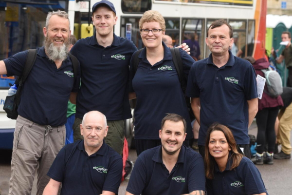
Exception PCB - The Five Valleys Walk 2019
|
|
|
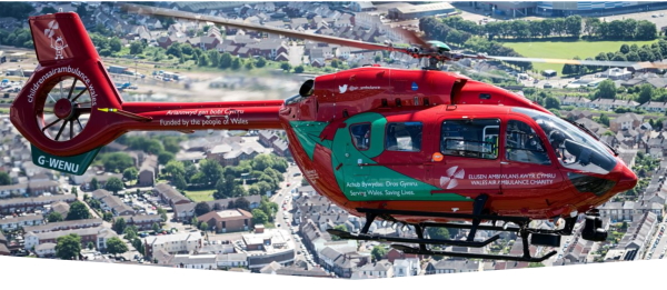
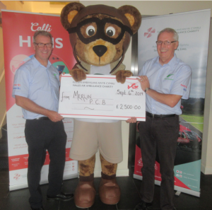
The Merlin golf open day had a charitable element and their suppliers and partners, a.o. Adeon, sponsored the events and raised money for the Wales Air Ambulance Charity. Merlin was very proud to hand over a cheque for £2,500 at the Wales Air Ambulance based in Caernarfon, North Wales. This is a fantastic response to a great charity; on the day of the presentation the helicopter ambulance was unfortunately called out which is testimony to the need for this service and the valuable work they do. Every mission typically costs £1,500 to put the helicopter in the air and requires annually £6.5 million to run. Although they were unable to see the helicopter, Biggles was there to accept the cheque. Nick McClean and Paul Machine presenting the cheque to Biggles. |
|
| Go back to Contents |