
Journal CSS

The Journal of The Institute of Circuit Technology Vol 14 No 1 March 2021 |
|
| Links to Contents | Section |
|
ICT Webinar: Novel Materials and Methods for Printed Circuit Fabrication |
|
|
3D printing of electronic systems for real world applications - Research Paper |
|
|
Industry News: Adeon, Amphenol-Invotec, Chasm, Eurotech, Trackwise, Ventec |
|
|
Section 1 |
Editors Introduction 2021 Collaboration and Innovation |
|
Lynn Houghton Journal Editor |
. As we enter this second year of Covid restrictions, we offer you a smorgasbord of innovation. We bring you a report on our second webinar with novel materials and methods, including the use of magnets and even spinach to further the green agenda. Jiva materials give us an update on the Recollect project, Soluboard and celebrate a €200,000 sustainability prize. We feature 5G developments and IIOT (Industrial Internet of Things) for increased connectivity. We have three papers demonstrating the collaboration between OEM, design, materials and manufacture. Also support from industry bodies, iNEMI and ICT. We have an interesting research paper on 3D printing combined with flexible circuits and assembly. I would like to thank all contributors, especially our new visitors Ericson and Leeds University, for their interesting contributions. |

|
Section 2 |
Editorial If They Could See us Now |
|
Bill Wilkie Technical Director - ICT |
The brief for the editorial was simple. No Brexit, Megxit or lockdown – and definitely no football. Annual Foundation Course then. The founding fathers of the course in 1980 would not have recognised today’s environment, but they were men of vision. At a time when the local population had never seen a napkin and thought metal cutlery was jewellery, they instigated a sit-down get-together dinner with all the trimmings and table linen not sellotaped to the table. The same high standard applied to the course materials, copies of every lecture in a gold blocked folder, which in some years amounted to 45 delegates and 6000 sheets – a good sized tree. Bill Wilkie |

|
Section 3 |
Calendar of Events |
|
Date |
2021 Events |
|
25th February 6th April - 27th May 1st June November |
AGM Webinar / Zoom Meeting Webinar Foundation Course Lectures Annual Symposium Webinar Evining Seminar and Facility Tour - Date to be confirmed |
|
|
|
Section 4 |
ICT Webinar: Novel Materials and Methods for Printed Circuit FabricationPete Starkey, I-Connect007 |
 |
For the first time since its foundation in 1974, the Institute of Circuit Technology had no alternative than to conduct its Annual General Meeting online. The event, which took place on February 25, 2021, was remarkably well-attended, and was followed, as is traditional, by a technical seminar. The seminar became a webinar focused on novel materials and methods for printed circuit fabrication and moderated by ICT Chair Emma Hudson. |
 CHASM Advanced Materials CHASM Advanced Materials |
The first presentation came from Tom Eldridge, business development manager with CHASM Advanced Materials, who gave an update on innovative transparent PCB materials for new markets. He commented that although indium tin oxide was established as the industry standard transparent conductor, dominating both glass and flexible market segments, its flexibility was limited, as was its transparency on plastic films, and it was not stretchable or formable. He listed as alternatives materials based on poly(3,4-ethylenedioxythiophene) (PEDOT), carbon nano-tubes, silver nano-wires, metal mesh, and carbon nano-tube hybrids. A proprietary hybrid of silver nano-wires and carbon nano-tubes was claimed to have better flexibility and formability than indium tin oxide, and to be more cost-effectively patterned. He showed examples of transparent flexible circuits patterned with this material. Fabrication and processing were straightforward, with minimal capital investment since most PCB shops already had the required equipment. The hybrid material was a combination of ink and film. It acted as a pattern mask and, being a functional part of the end product, remained in place without stripping. CHASM’s lab facility consisted basically of a screen printing press, a convection oven and a conveyorised etching machine. Transparent film, supplied pre-coated with silver nano-wires, was screen printed with carbon nano-tube ink, then dried and etched in ferric nitrate or ferric/cupric chloride to leave the required conductive pattern. Applications included transparent heaters, transparent antennas, transparent lighting films and transparent touch sensors. Eldridge gave a video demonstration of a side-by-side comparison of conventional UHF flex antennas versus transparent examples produced with the new hybrid material, illustrating that equivalent signal strength and quality were consistently maintained. Follow this link for the slideshow |
|
University of Dundee |
Spinach might be perceived as an unlikely accelerator for electroless copper plating, but was the subject of the next presentation—a nature-inspired project to examine ways of reducing the toxicity of electronic fabrication processes. Dr. Tom Jones from the University of Dundee discussed the development of an innovative photo-catalyst for selective plating on polyimide-based substrates for micro-patterning circuitry. Silver nanoparticles had been considered as a lower-cost alternative to colloidal palladium for catalysing electroless copper deposition, and these nanoparticles could be generated by photo-reduction of silver salts in solution. Research had indicated that the photosynthetic capability of chloroplasts present in spinach could significantly accelerate the photo-reduction reaction and yield a more effective catalyst for electroless deposition. Selective LED exposure of a surface pre-treated with ionic silver and sensitised with an alcoholic extract of spinach offered a photo-imaging process for creating circuit patterns in catalytic silver nanoparticles that could be subsequently built up with electroless copper. Dr Jones showed examples of patterns on polyimide substrates. A study of the mechanism of the photo-reduction reaction, using pure chlorophyll in place of spinach extract, gave anomalous results—the spectral peaks did not match. Further investigation revealed that potassium chloride was present in the spinach extract, and this was in fact the active ingredient rather than the chloroplasts themselves. X-ray diffraction analysis indicated the presence of silver chloride in the spinach-activated ionic silver surface coating, which was a reaction product of ionic silver with potassium chloride that had originated from the spinach. Jones pointed out that silver chloride was a typical light-sensitive constituent of traditional photographic film, and this explained its contribution to the photo-sensitisation process. Follow this link for the slideshow |
|
Coventry University |
Selective metallisation of textiles using a magnetic field was the theme of a research project at Coventry University, presented by Dr. Sofya Danilova. The objective was to find a lower-cost shorter-process-route alternative to lithography, avoiding hazardous chemistry and wastage of materials. It was proposed to use a magnetic template to define a circuit pattern in a catalytic material, and then build it up using electroless deposition. Traditional catalysts based on colloidal palladium or colloidal copper were not magnetic, so an alternative was required. A colloidal composite of metallic silver as the active component and iron oxide as the magnetic component was found to be effective. Magnetic deposition conditions had been optimised and Dr. Danilova showed examples of electroless copper plated onto thin FR4 material, areas of which had been activated using this catalyst. Dr. Danilova demonstrated the use of templates, designed using software to simulate magnetic field distribution, and showed scanning electron micrographs of 500 micron lines produced in electroless copper. Woven polyester fabrics had been selectively metallised using the magnetic technique, although the pre-treatment of the textile had been shown to be an important consideration, as had the stirring method--magnetic stirrers were not recommended! The research had successfully demonstrated proof of concept, and future work would be directed at reliability testing of metallised textiles and investigating the properties of metallised textiles with high surface area. Follow this link for the slideshow |
|
Emma Hudson brought the proceedings to a close, thanking the contributors and all who had attended, and especially ICT technical director Bill Wilkie for his expert organisation of the event. She was optimistic that the Institute could soon return to its live seminar programme. Published by kind permission of Pete Starkey, I-Connect007 |


|
Section 5 |
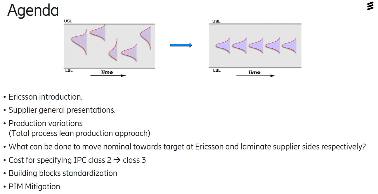
5G+ Readiness and Challenges Stig Källman |
|
Introduction: It is my pleasure to be writing this introduction to Stig Källman’s piece on “5G+ Material and process readiness and challenges + 2020”. I have had the opportunity to see Stig present on Ericsson’s Material Tool Box on two occasions now and I find it fascinating; to me, it would seem to be a common sense approach for designing and producing a quality product. This Ericsson presentation walks you through some of the manufacturing challenges faced with 5G products and how understanding the material’s properties are critical to this. The key messages I took from Stig Källman, when he kindly walked me through this, were – • Characterisation of the material properties are critical and the consistency of the properties and the measurement of them is fundamental to the 5G products (and 6G development). Stig left me with a great example of how consistent they need their materials to be, he told me to think of a Big Mac and how wherever you order this in the world, all of the ingredients used to make it are the exactly same. That is the level of consistency needed with the materials for 5G products. I’d like to thank Stig Källman and Ericsson for their contribution to the ICT Journal. If any of our readers have any questions for Stig then please let the Journal team know and we will pass these on. Emma Hudson, ICT Chairman |
|
|
|
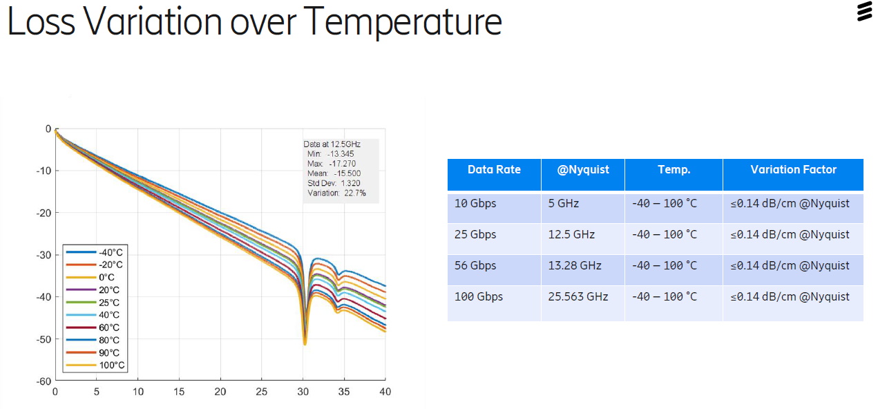
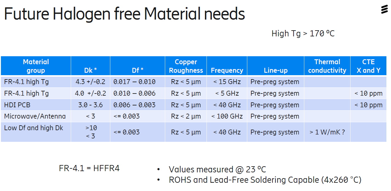
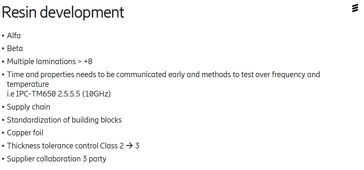
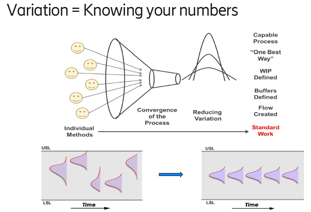
To be prepared for future challenges the need for thinking modular and about possible parameters to standardize is critical to have a design that can be copied and reused into all factors that can be identified and set as “K” constant. Of course, all K´s will have a variation but then by measuring where you are today is a starting point of feeding this requirement both up stream and down stream. Starting like this would make you start at one level and continue to improve the production processes that makes your PCB a more robust and better performing product. The data can be inputted into the simulation tools to predict the performance according to the “real” production By take that in consideration the design can be adopted to the best circumstances in the PCB production so the lines can be run at the most optimum and with this the best yield and cost.
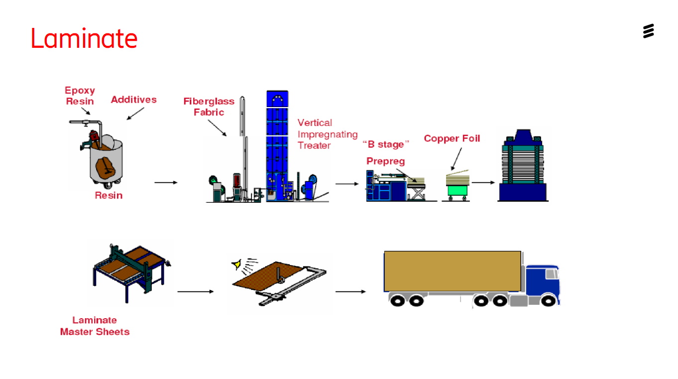
The laminate processes. - By using the IPC appendix list for standard constructions and apply that to your standard build-ups you will get the material that is mostly produced with the lowest variation and lowest cost. Also using 1 ply approach for B stage makes a lowest cost at start.
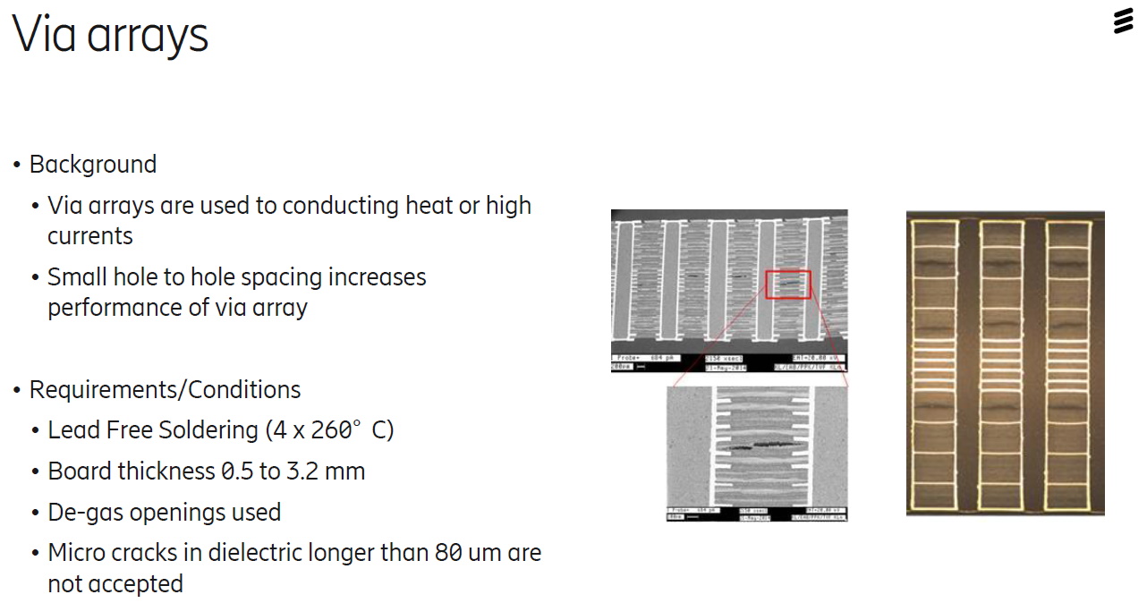
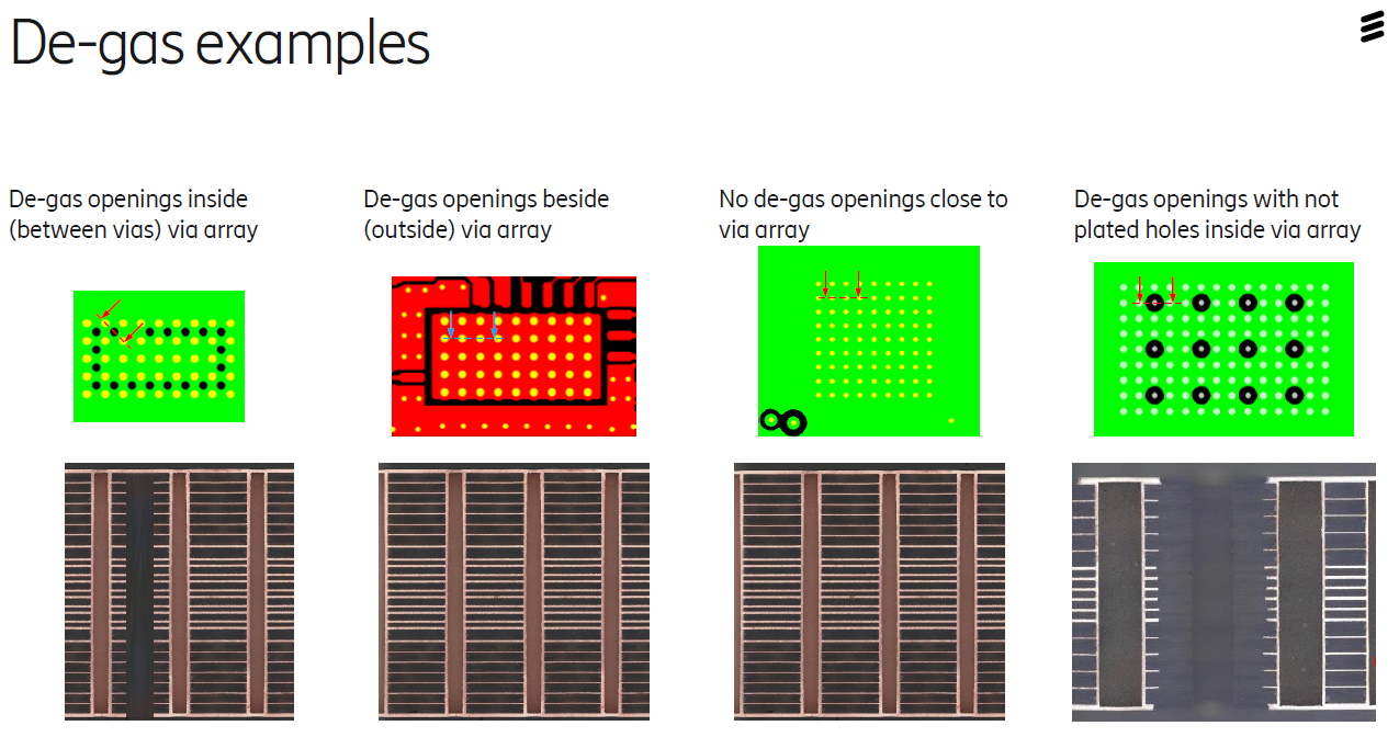
In addition the use of via hole arrays makes the material weaker at local areas and to have a material that is not so brittle is important for any future process as drill, de-smear and future lead free reflow processes.
The design must also be adapted for enhanced moisture escape. So here the property of the water absorption that makes the material easy to breathe is a key factor for survival of reflow processes. Thus the designers also want to place the holes as tight as possible together to increase the thermal conductivity through the holes.
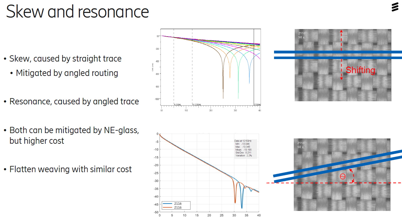
By choosing a square weave or with the same amount of bundles in both directions enables good performance in the signaling of the board.
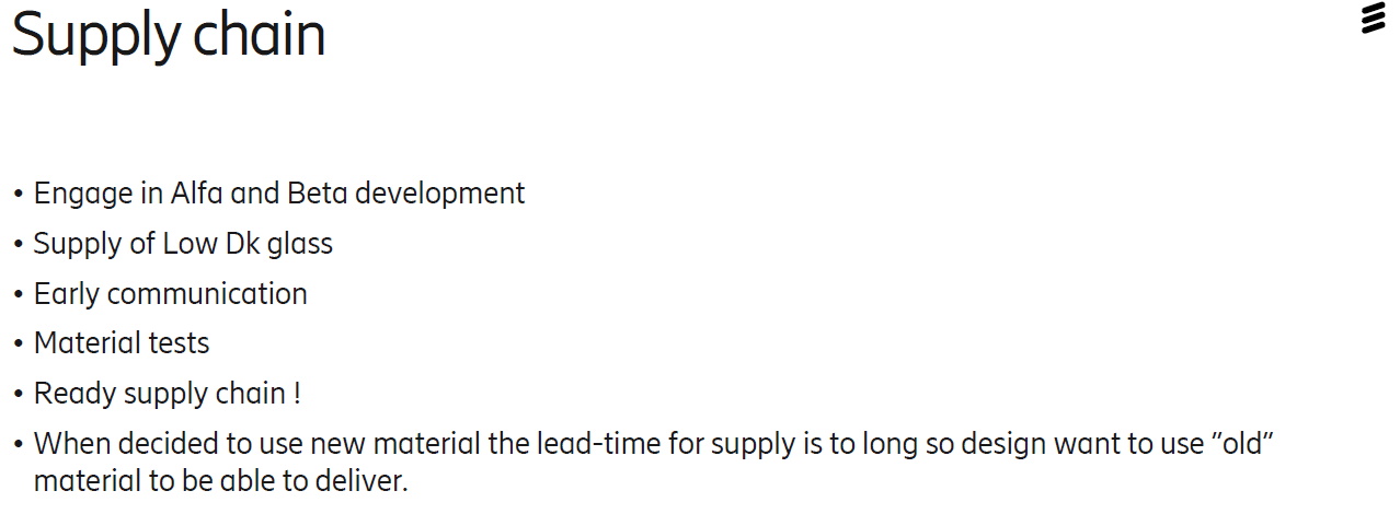
Above all things it is important to engage at an early stage with the PCB material suppliers to be able to test and evaluate during R&D process.
A new material is only useable after the PCB supplier knows how to process it and a supply chain is working at volume levels. Otherwise the PCB supplier will have to suggest alternative material to ensure the customers delivery lead times are satisfied.
Have annual meetings with your suppliers and keep a focus on the performance from todays measurements while driving activities of continuous improvement. The results can be measured and additional requirements can be added without disrupting the process of progress.
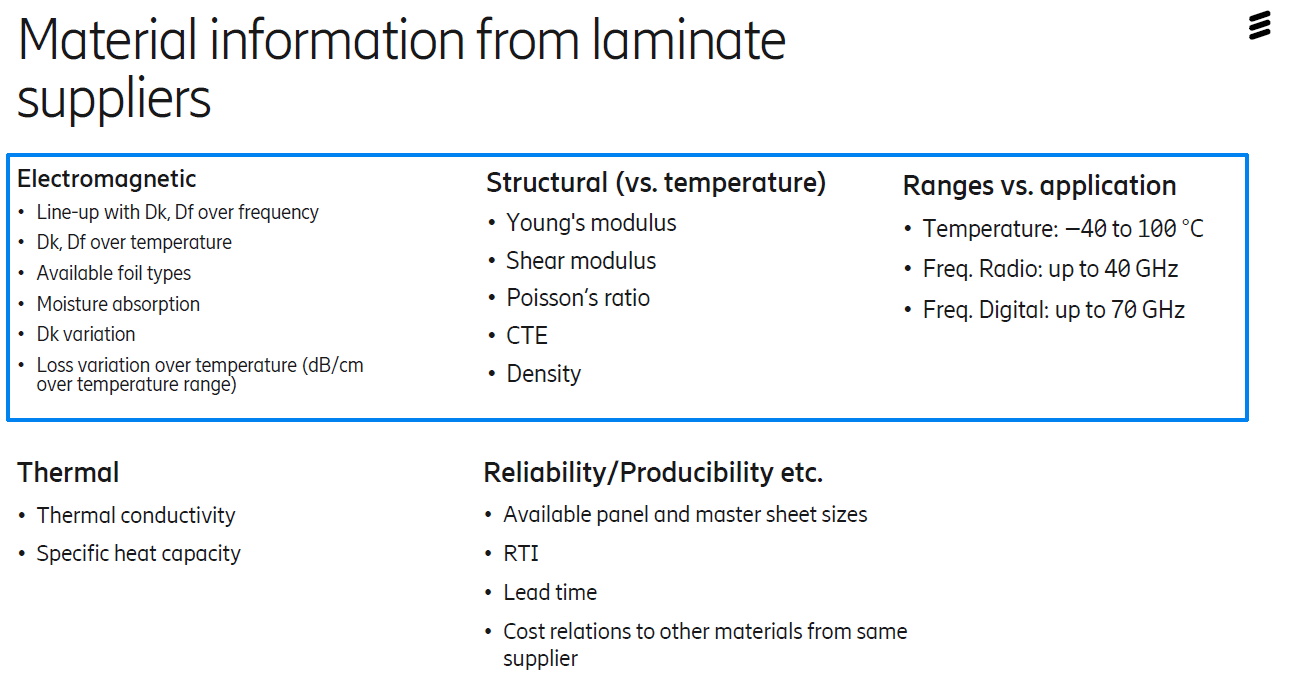
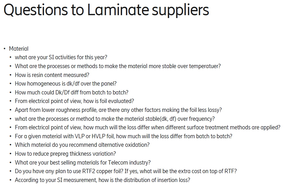
The above questions are collected from the design community to help the laminate manufacturer make their specification of the product much better. Also, as a final word of future standardization of copper foil. Its not enough adding additional abbreviations like RTF3, HVLP2 etc. The designers must have a clear way to specify the product and also supporting second source material. The PCB supplier must be able to measure the requested properties delivered in μm.
|
| Go back to Contents |
 Stig Källman
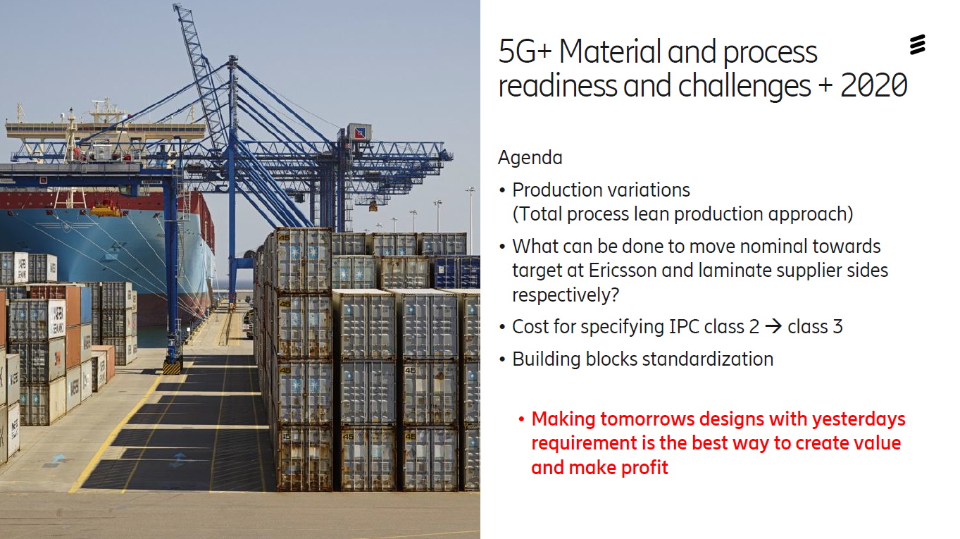
|
Section 6 |
5G Driving High-Performance Material Demand Alun Morgan |
|
|
Many aspects of work and life are set to be revolutionized by the global rollout of 5G as a critical enabler for connected cars and self-driving vehicles, autonomous factories, remote medical surgery and the diffusion of smart “things” throughout cities, infrastructures, and our homes. The impact on the automotive sector alone promises to be huge thanks to attributes like ultra-low latency that will enable time-critical use cases such as V2X. The 5G Automotive Association (5GAA) is excited about the prospects for cellular V2X (C-V2X) to consolidate vehicle-to-vehicle, vehicle-to-infrastructure, vehicle-to-pedestrian, and vehicle-to-network modes combining direct communication, communication with cell towers, and links to cloud services. For a country to delay 5G rollout risks compromising standards of living and economic competitiveness. On the other hand, concerns about foreign involvement in such a pervasive infrastructure are widely reported. It’s very clear what’s at stake. The fear of falling behind is driving the search for solutions. Moreover, in the race to unleash the benefits of 5G for life, work, and everything, we can expect increasing pressure on the pace of intellectual-property development as well as demand for the high-performance components and materials needed to make it real. |
|
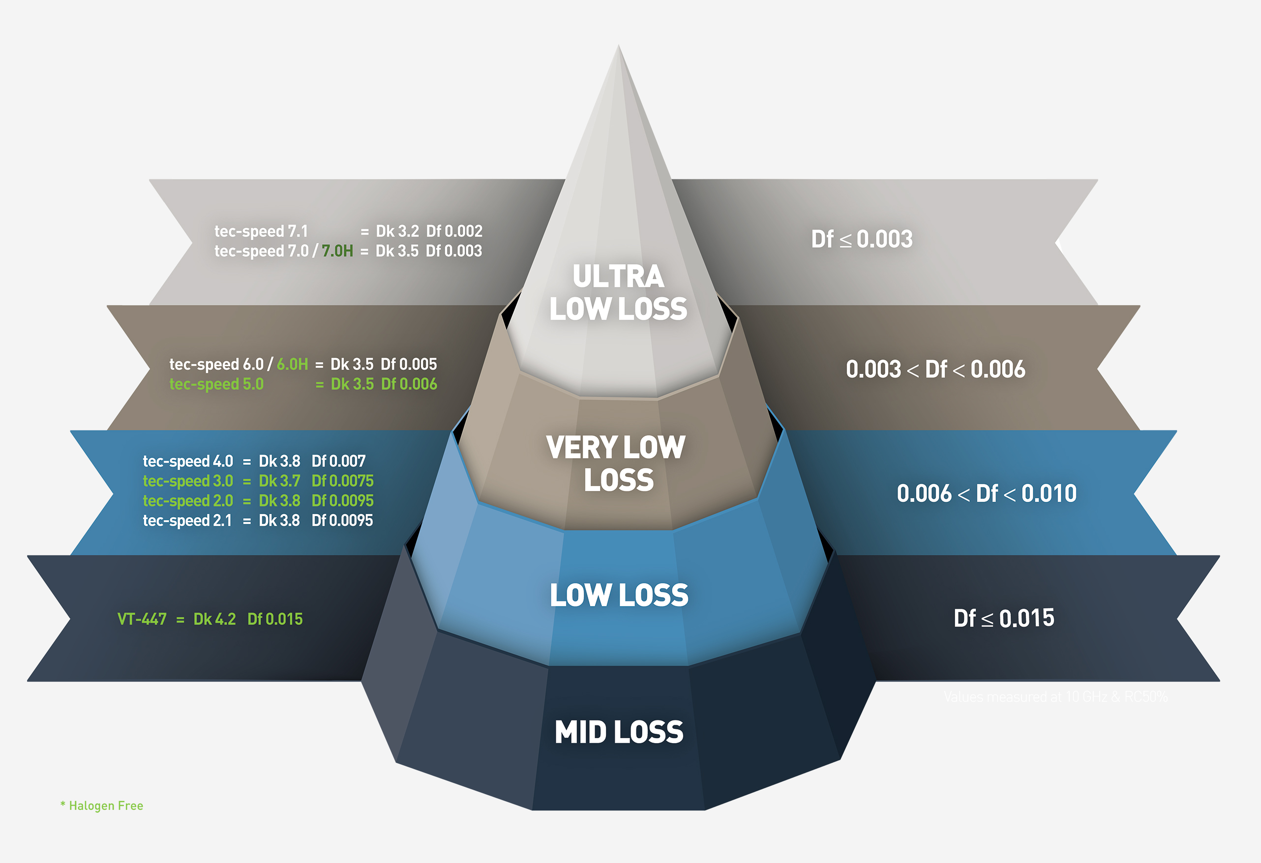
Fig 1: Tec-speed high-speed material technology – the ultimate choice for high-reliability and high-speed applications |
|
|
The PCB substrate materials capable of satisfying 5G technical specifications are esoteric, high-performance formulations characterized by very low losses. Tightly controlled dielectric constant (Dk) and low dissipation factor (Df) are needed to ensure signal integrity and minimize power demand and heat dissipation. Low passive intermodulation and good thermal stability are also required. The materials are technically specialised, few companies can produce them, and supply can be limited. 5G infrastructure rollouts have barely hit their stride and already there is talk of shortages that could delay and disrupt projects ongoing around the world. Applications like 77GHz automotive radar, also, are set for explosive growth and so will compete for a share of the supply. |
|
|
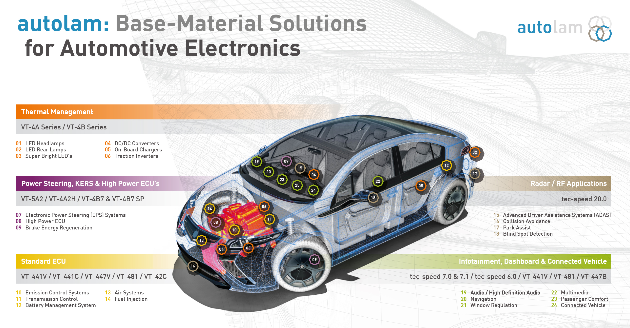
Fig 2: Autolam base material solutions - high performance automotive electronics begins with innovative materials |
|
|
Part of the problem is that manufacturers of substrate materials are managing complex, globalized supply chains that are difficult to control. There are many variables and some companies in these chains may have conflicting business interests. Ventec’s wholly-owned supply chain provides protection against some of these hazards. Lines of communication are kept short and we are not dependent on the supply-chain management skills of third-party companies. No company has unlimited resources or flexibility to be able simply to ignore the effects of global supply shortages that coincide with surging customer demand. However, when you have complete control over the means of production and distribution it’s easier to make relatively small but influential adjustments to handle the situation. You can increase production capability and capacity in targeted locations, increase stockholding of the most affected products, and distribute inventory in strategic locations globally. On the other hand, the understanding and cooperation of customers is vital to be completely confident of delivering the required products, to the right place, at the time they are needed. Ideally, this should extend to automated electronic cooperation between the supplier’s and customer’s enterprise resource-planning software tools. Letting the machines share the information they need automatically is the most effective and efficient way to ensure customers’ needs are communicated properly to be fulfilled at the right time. On the other hand, human interaction is very much needed at the cutting edge of product development. The technical demands in cellular infrastructure are always ahead of the standards-making processes, so equipment designers need to work extremely closely with their material suppliers to be sure they are utilizing the latest materials available and to make their products as good as they can be. |
|
|
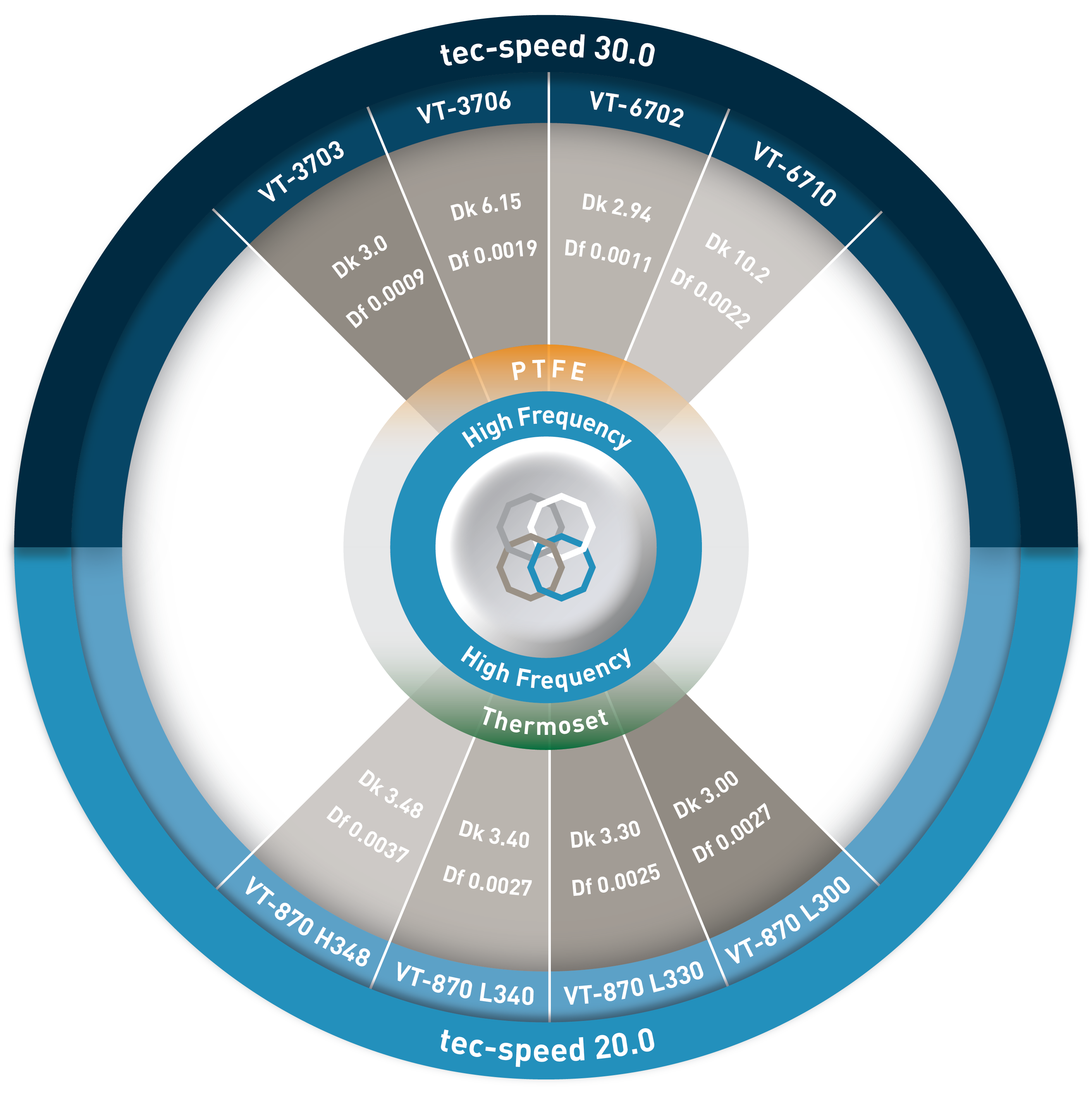
Fig 3: Tec-speed high-frequency material technology – the ultimate choice for high-reliability and high-frequency applications |
|
|
There is an important change in the standards landscape, however, concerning the latest specification IPC-4103 that covers low-loss materials for use in printed circuits for microstrip, stripline, and high-speed digital circuits. Unlike specifications like IPC-4101 and IPC-4921, which were derived from NEMA specifications first published in the 1960s, IPC-4103 characterizes materials based on their Dk and Df at different frequencies without concern for chemical composition. Materials covered by this specification typically have Df less than 0.005, such as Ventec’s tec-speed 20.0 materials that have Df as low as 0.002. There is little doubt that the performance of modern PCBs has advanced significantly since the 1960s, so it makes sense to bypass the constraints of 1960s thinking when it comes to material grades. After all, the PCB designer cares only about performance of the PCB and the PCBA. At Ventec, we have sought to help designers focus on performance by bringing together specially curated groups of products that are suited to specific application areas. One example is our autolam solutions set, which presents a small number of materials that are pre-selected for automotive use cases such as under the hood electronics, infotainment, and lighting to save designers searching hundreds of IPC-4101 specification sheets for a suitable grade. Either way, emphasizing performance over composition enables a pragmatic approach to material selection that should make all our lives easier. |
|
| Go back to Contents |
|
Section 7 |
iNEMI Projects and Initiatives Address 5G/mmWave ChallengesUrmi Ray and Steve Payne |
|
Steve Payne
Urmi Ray |
The International Electronics Manufacturing Initiative (iNEMI) is a not-for-profit R&D consortium of approximately 90 leading electronics manufacturers, suppliers, associations and universities. iNEMI roadmaps future technology requirements in electronics manufacturing, identifies and prioritizes technology gaps, and helps eliminate those gaps through collaborative projects. These projects leverage the resources of participating member companies, reducing the risk and cost to any one organization. The most recent iNEMI Roadmap highlighted the adoption of 5G/mmWave technologies and accompanying disruptions to design, materials, assembly processes and test protocols that can directly affect PCB design and fabrication. iNEMI has instigated new collaborative projects and initiatives to address these challenges. 5G/mmWave Materials Assessment and Characterization Project Reliability & Loss Properties of Copper Foils for 5G Applications Project To mitigate signal loss due to rough copper surfaces, very low-profile copper foil is available, but this in itself can challenge some traditional test methodologies. New (non-contact) techniques of copper profilometry are available and are already referenced in IPC TM650 2.2.22. In addition, IPC 4562 is being updated to include development in copper foil technology and to provide standardized quantitative nomenclatures. A further consideration for low-profile copper foils combined with low loss dielectrics is the traditional method of measuring bond strength of copper foil to dielectric by peel testing, which may not always be indicative of the durability and reliability of multilayer printed circuits. It is against this background of new PCB material developments and metrology techniques that an informed and comprehensive study is being undertaken to support current and new standards and to provide complementary and supplementary empirical data for meaningful characterization of materials. Guidelines will be produced to support the design process to ensure that PCB electrical performance criteria are met while exhibiting the required durability for demanding applications. For more information on any of the topics described in this article please contact Steve Payne ( Authors: Urmi Ray and Steve Payne
|

|
Section 8 |
ReCollect - Efficient Manufacturing of Recyclable Composite Laminates for Electrical Goods – No 34163 Bill Wilkie |
|
DISSEMINATION NEWSLETTER 2020 The ReCollect project is funded by Innovate UK, part of UK Research and Innovation. It began in October of 2019 and is intended to run for 30 months. Normally, the ICT would be holding events which could be used to disseminate the latest information on the project, but during the Covid-19 lockdown, we are using this on-line vehicle to ensure that the Industry is kept up to date. Innovate UK is the UK’s innovation agency. Innovate UK works with people, companies and partner organisations to find and drive the science and technology innovations that will grow the UK economy - delivering productivity, new jobs and exports. The aim at Innovate UK is to keep the UK globally competitive in the race for future prosperity.
PARTNER ORGANISATIONS LEAD PARTNER Established in September 2017, Jiva Materials Ltd is a sustainability start-up based in London, UK. Jiva, as the inventor of Soluboard, will lead the specification and development of the thermoplastic input materials, as well as the conversion of the substrates into working circuit boards. Jiva will also coordinate the project.
DEVELOPMENT PARTNER Coventive Composites is a specialist independent consultancy, providing technical expertise and access to pilot-scale equipment and testing facilities to help our clients develop and commercialise novel composite materials and components. Our expert advice and technical support cover all aspects of the product development lifecycle.
DISSEMINATION PARTNER The ICT facilitates dissemination of knowledge and expertise by a series of seminars and symposiums in varying locations throughout the UK. The ICT Quarterly Journal contains papers and information regarding novel processes and techniques and they also offer an annual Foundation Course in PCB manufacture and design. This is a valuable source of information for both novices and more advanced engineers wishing to widen their knowledge and experience of the application of cost effective and reliable processes and techniques.
Review of progress at our last evening event At the end of the second quarter, Dr Jonathan Swanston, chief technical officer with Jiva Materials, gave an update on the ReCollect project and explained the background to the development of the world's first fully recyclable PCB laminate. He passed-around samples of his material, composed of a natural fibre bound with a polymer soluble in hot water but not in cold water, which had the appearance of a light-brown-coloured unclad laminate. Dr Swanston reviewed some statistics which indicated that PCBs made up 8% of the 50 million tonnes of electronic waste that was generated in 2018. The ReCollect project explored an alternative way of managing end-of-life circuit boards. Currently, the only practical way of recycling glass-epoxy circuit boards involved shredding and incineration to recover the metal content. The ultimate aim of the project was to remove glass-epoxy boards from the supply chain, by demonstrating that Jiva’s Soluboard® could match the performance of CEM-1 and FR-4 materials. He explained that Soluboard® was a fully biodegradable and non-toxic product based on flax. A primary aim of the project was to demonstrate the feasibility of producing the material in high volumes at a competitive price, using a continuous-production process in development by Coventive Composites. The nature of Soluboard® was to delaminate when immersed into hot water, enabling the flax fibres to be composted or repurposed and the electronic components to be removed for re-processing. Silver printing was a feasible method of creating functional circuits, but in order to use existing aqueous manufacturing processes it was necessary to seek a means of chemically protecting the material in-process, and this was part of the project. Dr Swanston commented that “white goods” – large household appliances – constituted more that 30% of e-waste, and that the Global E-Waste Monitor had reported that less than 20% of this was documented as collected and recycled. The rest went to landfill. Jiva intended to push for the safe recovery of e-waste in line with the WEEE2 Directive. The white goods market was their initial target, and specifications from potential customers had defined electrical, flammability and mechanical requirements. Soluboard® had a Tg of 126°C and a UL94V0 flammability rating. Its electrical properties were being determined by a third-party laboratory and final results were awaited. As part of the project, functioning populated PCBs would be designed, manufactured and evaluated as specified by end customers. We intend to update this newsletter as monthly link to our website as a way of keeping the project in the Industry's in-tray, during the lockdown.
FIRST QUARTER 2021 Much has happened recently, including a Zoom Dissemination Webinar, where Jonathan Swanston of Jiva Materials was able to update an interested group of delegates from the Fabrication and Supply sectors of the electronic Industry. A write up of the presentation was prepared by ICT Recorder, Pete Starkey, who also arranged for a copy of the write up to appear in the prestigious on-line technical Journal, PCB.iconnect007. The project was also brought to the attention of Delegates at our ICT AGM Meeting in February
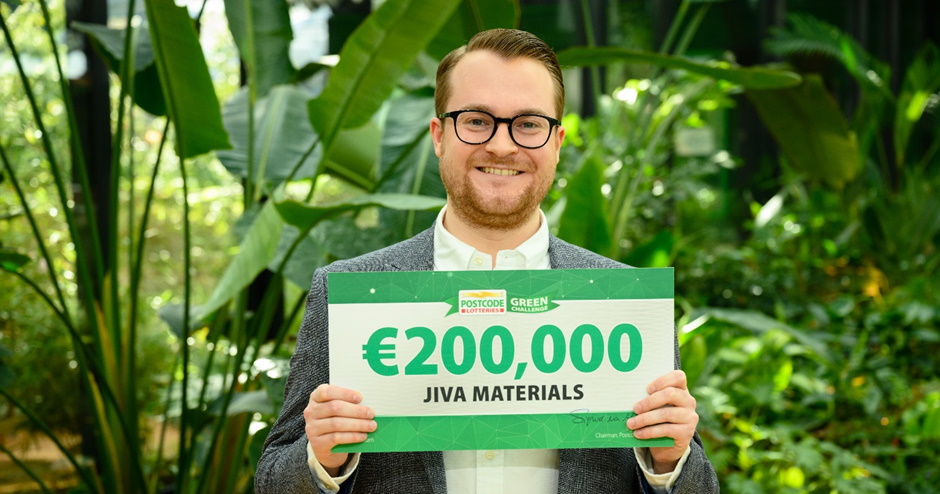
LATEST NEWS 25.02.2021 Jiva Announced as Runner-Up in Postcode Lotteries Green Challenge
Jack Herring, Jiva CEO receiving his award. On the evening of 24th February, it was announced that Jiva had been selected as the runner-up of the Postcode Lotteries Green Challenge 2020 on a Dutch TV show watched by 2 million people. The TV show titled 'Iedereen Kan Het' or ‘Anyone Can Do It’ was broadcast by Omroep Max. It showcased all six finalists of the competition, highlighting the problem that each of the start-ups are tackling and presenting their sustainable innovations for the future. Jiva was one of the two UK start-ups in the finals, with both of them securing the first and second prizes of €500,000 and €200,000 respectively. There was also more than just the two companies’ locations that they have in common, with Jiva CEO and co-founder, Jack Herring, and the founders of SoluBlue, Ayca Dundar and Francis Field, all being alumni of the Royal College of Art in London. Over 650 start-ups applied to the Postcode Lotteries Green Challenge 2020, from countries including the UK, the Netherlands, Sweden, Norway and Germany. The Green Challenge fund is managed by the DOEN Foundation, a Dutch non-profit organisation which also connects parties in its network to assist the finalists following the award of the prize money. During the TV show, Jack engaged with the Dutch scientific journalist and presenter, Anna Gimbrère, as well as the CSR manager for KPN, Brechtje Spoorenberg. KPN is a Dutch telecommunications company that is focusing on the circularity of their electronic and electrical products. The company states that they are already recycling 80% of their TV receivers and modems, with a target being set of achieving 100% circularity by 2025. This is an attempt to help contribute to the Netherlands’ goal of achieving a truly circular economy by 2050. Jiva will be using the competition winnings to continue expanding their new pilot facility in Waterlooville, Hampshire. This will enable the company to demonstrate the utility of Soluboard to potential customers, transferring many of the production processes from third party facilities in-house. Jiva will also use the funds to finance to produce their initial batches of Soluboard for prototyping projects with potential customers. Securing second prize in one of Europe’s most prestigious sustainability focused competitions is validation of Jiva’s novel solution for the fastest growing waste stream in the world – electronic waste or ‘e-waste’. The international recognition will provide Jiva the platform that is required to publicise this huge problem and position Soluboard as a commercially viable solution. Jiva is now preparing for fundraising, planning to fulfil a seed investment round later in 2021. Further investment will allow the UK based company to collaborate with more of the world’s leading electrical and electronic equipment producers. Jiva would like to hear from any potential customers who feel that Soluboard would be a good fit for their portfolio.
|
|
| Go back to Contents |
|
Section 9 Research Paper |
3D Printing of Electronic Systems for Real World ApplicationsRobert Kay and Matthew Shuttleworth |
|
Robert Kay
Mathew Shuttleworth |
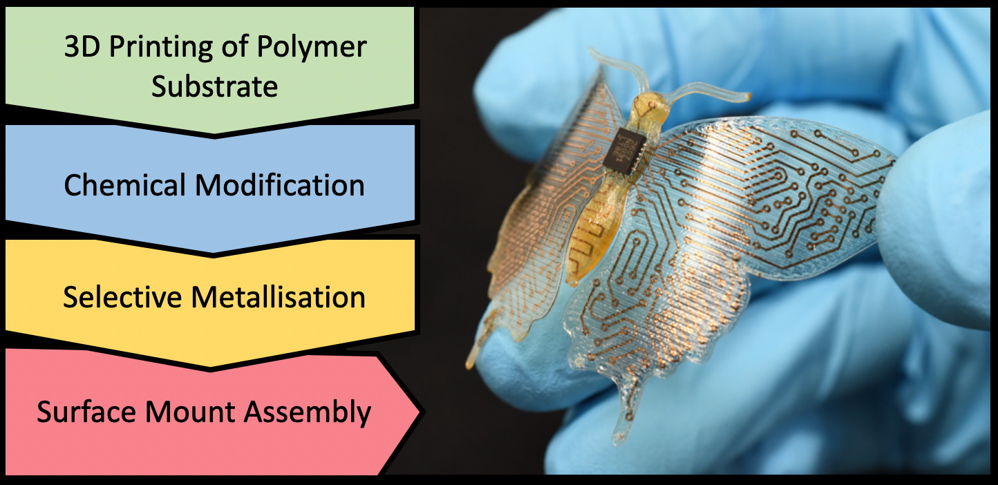
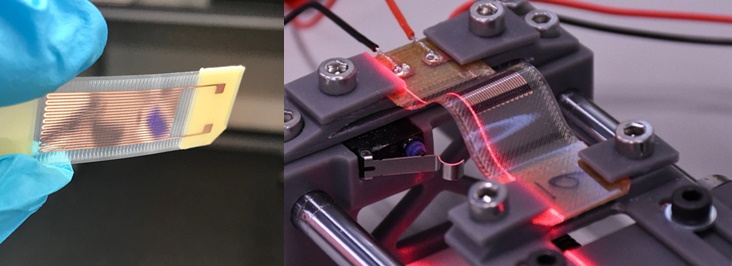
Introduction Additive Manufacturing also known as 3D Printing has been forecasted to revolutionise the way we design and make products with industries such as medicine, aerospace and automotive finding ever increasing applications. Based on the concept of successively adding material to create a 3D object straight from a computer model, Additive manufacturing offers advantages over traditional production methods by allowing highly geometrically complex and personalised products. However, 3D Printing techniques have made limited inroads for the production of electronic systems since improvements in processes and materials is needed to achieve the resolution, performance and reliability required to allow real world applications. This article summarises the recent collaborative research by the University of Leeds and Heriot-Watt University focused on developing an Additive Manufacturing based process for achieving high-density circuitry that is compatible with advanced packaging techniques. The process involves a 4-stage approach as shown in figure 1. To demonstrate the geometric design potential of this technique a 3D butterfly shape with 59mm wingspan was manufactured.
Figure 1: Process flow and resultant visual demonstrator produced using this technique
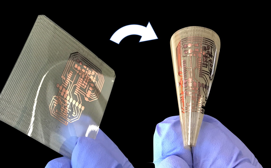
The Manufacturing Process 1) 3D Printed Polymer 3D circuitry
Figure 2: Highly flexible circuitry Figure 3 – 3D printed rigid and flexible substrates
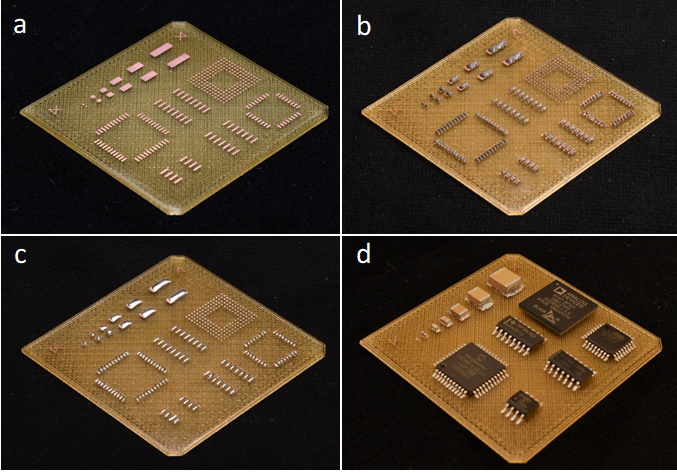
Solder based Surface Mount Packaging A restriction for the manufacture of electronic systems using 3D printing is the methods for packaging components. Due to the low temperature capability of the printed polymer, or the poor solderability of the conductor material, techniques have primally relied on bonding using lower temperature joining materials such as conductive adhesives. The combined properties of PEI having a high heat capability and the wettability of copper allow investigating the potential of attaching surface mount components to the 3D printed substrate using solder interconnects.
Figure 4 – a) 3D Printed test board showing Cu pads, b) SAC solder dispensed through a 0.21mm ID nozzle, c) solder reflowed showing wetting to the Cu, d) range of surface mount components soldered to test board.
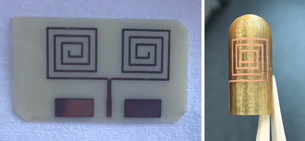
The properties of the dielectric PEI substrate and copper conductive traces allows the exploration of high frequency wireless applications. Additive Manufacturing based approaches offer the geometric flexibility allowing RF engineers to consider 3D shaped antennas. Using this manufacturing method, a dual spiral monopole antenna connected in parallel was manufactured in both a planar and 3D format, Figure 5. The 3D pill capsule shape offers a more compact format while also offering a wide solid angle coverage.
Figure 5: Flat versus 3D conformal antenna. Pill capsule diameter 11 mm, 0.8mm shell thickness, 0.4 mm conductor track width Looking to the future This article has summarised a new 3D printing based process that allows the production of high-resolution conformal and flexible electronic circuitry on 3D printed substrates. This 3D manufacturing approach offers new designs freedoms through the precise placement of high performance electronic materials and offers a route to increased customisation and device functionality. In the future closer integration of mechanical and electronic systems could be achieved through embedded data processing, communications, sensing and power transfer. The process resolution & performance opens up routes to produce mass-customised medical devices, personalised wearable technology and bespoke robotic systems. However, challenges still exist for the creation of 3D Printed electronics. Currently the design process is ad hoc and not aligned to existing multilayer circuit design. Furthermore, processes must be able to validate the same reliability of mass-produced electronics systems through extensive accelerated age testing. At present, standards do not exist for 3D Printed electronics, but with continued process and material, the industry will be able to align conventional electronics manufacturing methods to allow the seamless transition using 3D Printing based techniques. Video Presentation A video showing the manufacturing and process operations can be viewed here - Follow this link to the video
|
| Go back to Contents |


|
Section 10 |
PCB Fabricators Group - a Benefit to all who Fabricate PCB’s in the UK. |
|
Matthew Beadel |
The Fabricators group met in early march for the first of its 4 meetings in 2021 – the group may even be able to meet in person later in the year? The turnout for the meeting was again very good with over 60% of the members attending, very promising as many Fabricators are currently very busy. The 2 hour teams meeting followed the standard format of Francesca Sterns B2B Industry report followed by various agenda items from disaster recovery (how the group can assist) to suggestions for lobbying of Government - finishing with the ever popular round table discussions. The main items taken away from the meeting were concerns over sporadic material price increases, further issues over shipping to and from Europe created by BREXIT and the continued concerns from COVID both within fabricator sites and the external issues such as Service engineers travelling from Europe. But there was also a degree of positivity, where many off the sites felt business was improving and there was a light at the end of the tunnel – even if it was still quite a way off! If any fabricators are not currently members of the group and would like to get involved in the helpful and informative discussions, please let either Bill Wilkie know or contact the Fabricators group directly. We are always happy to welcome new members to the group, as we feel we are stronger together. |
|
Section 11 |
Industry News |
| CCI Euolam and Adeon |
CCI Eurolam Group SA Signs Agreement to Acquire Adeon Technologies BV CCI Eurolam Group SA, a leading distributor and industrial service provider to the EMEA electronics manufacturing industry, announced the signature of an agreement to acquire Adeon Technologies BV, a major full service provider of equipment for the European PCB Industry. Alain Kahn, President of the CCI Eurolam group: “we are thrilled to welcome Adeon into the CCI Eurolam family. The current context shows a strong dynamics regarding manufacturing and we are excited to participate and support the favorable industrial investment trend in the EMEA region.” Samuel Bismuth, Business Development Manager at CCI Eurolam Group commented: “There is a strong strategic fit between our companies and with the support of the CCI Eurolam Group, Adeon will keep strengthening its capabilities to expand and accelerate its growth. We believe that in the next decade, Equipments will be more than ever a strategic driver for technology in the electronics manufacturing industry and that Adeon is the right partner for the future.” Andre Bodegom, Managing Director and owner of Adeon said, " At Adeon, we have been able to develop over the last 10 years a strong expertise in selling and servicing equipment over the EMEA region partnering with leading equipment manufacturers. As we started discussion with CCI Eurolam, it immediately became apparent that both healthy companies have a lot to offer to each other. The European PCB market is developing rapidly into various highly specialised companies, for which the combined expertise of CCI and Adeon will create a lot of Added Value. Becoming part of the strong and renowned CCI Group of companies will allow us to materialise our growth plans for the future in an even faster pace. Adeon will continue to operate from its base in Breda, The Netherlands in a business as usual manner." |
| Amphenol-Invotec |
Amphenol Invotec secures £2m defence contract for the supply of PCBs This award further cements the company’s position as one of the leading supplier of PCBs to the defence market. Amphenol’s capabilities are among the world’s broadest and most advanced, delivering consistent quality and reliability for mission-critical applications. Read more.... |
| Chasm |
Flexible Screen Printed Conductive Inks While carbon nanotubes have long been regarded as a "miracle material," their benefits have been difficult to realise in the absence a practical manufacturing platform. The development of CHASM's V2V (Viscous-2-Vapor) ink technology provides such a platform. CNTs, remaining dispersed in V2V, can be easily screen printed using existing technology to facilitate the development and manufacturing of a broad range of transparent conductive film solutions. For applications where transparency, conductivity, AND flexibility are all required this platform is creating a new material category—Flexible Hybrid Transparent Conductive Films. Read more.... |
| Eurotech |
Eurotech - Brexit Update Further to the recent news of a trade deal with the European Union (EU), we are pleased to confirm that there will be no taxes on goods (tariffs) or limits on the amount that can be traded (quotas) between the UK and the EU from 1 January 2021. There are some alterations in the documentation required but these have been put in place and at present we can see no complications for our customers. As far as our European customers are concerned it is very much ‘business as normal’.Read more.... |
| Trackwise |
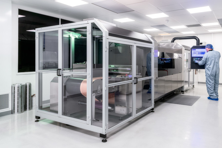
Tewkesbury, UK: Trackwise, a recognised innovator of flexible printed circuit (FPC) technology, continues to strengthen its production capability and capacity by investing in new equipment. The company has installed a highly advanced roll-to-roll direct imaging system and has also invested in a roll-to-roll flexible circuit laser drilling system.
|
| Ventec |
Ventec UK Maintains Highest AS9100 D Quality Compliance We are pleased to announce that our European headquarters in Leamington Spa, UK continues to maintain highest AS9100 Revision D compliance in accordance with the Aerospace Supplier Quality System Certification Scheme following successful completion of its surveillance audit. Our locations in the UK and China are certified with AS9100 Revision D and our German facility will follow shortly.Read more.... |
| Go back to Contents |
| Section 12 |
Members News |
|
Paul Brazier Obituary |
A former BT colleague has recently informed me that Paul Brazier passed away at the end of February. I am told that this was due to bowel cancer. I estimate that he was aged about 70. Paul had a significant role in the 1980s as the key player in the BT approvals schemes for the PCB fabrication and assembly industry. The UK telecoms infrastructure was updating from electromechanical switching to analogue and then digital switching. Millions of PCBs were required; most of which were manufactured in the UK. The System X ‘subscribers’ line card’ could be seen in production the length and breadth of the country. The approvals also included base laminate, solder resists, conformal coatings and assembly fluxes. Those in our industry who recall Paul will know that he was part of a team that included Bill Stace, Brian Stevens, Steve Clee and eventually myself. I have lost contact with Paul since leaving BT and so I am unable to provide any current family details, but I thought that this brief information would be appreciated by those in our industry who interacted with him. Len Pillinger March 2021 |
| Go back to Contents |
|
Section 13 |
Membership News |
|||
|
13.1 |
Membership Update |
|||
|
Technical Director and Membership Secretary |
NEW MEMBERS SUMMARY 2020 |
|||
| Membership No | Name | Company | ||
| Fellows | ||||
| 10477 10478 |
Philip Johnston John Priday |
Trackwise Teledyne Labtech |
||
| Members | ||||
| 10491 10492 10493 10494 10495 10496 10497 10498 10499 10500 10501 10502 10503 |
John Kear Melanie Berry John Li John Smith Kamal Berberi Adam Wellington Shaun Walker Alan Millard Alan Good Jonathon Meadows Gary Byrne Garth Allison Diane Sutton |
CCE CCE Exception Graphic Exception Graphic Merlin pcb Stevenage Graphic Stevenage Merlin pcb Merlin pcb CCE |
||
| Associates | ||||
| 10479 10480 10481 10482 10483 10484 10485 10486 10487 10488 10489 10490 |
Silver Merkoci Zbigniew Polak Ryan Kyle Jason Price John Gover Matthew Baines Lewis Wrigglesworth Elana Neascu Gauthier Gerardin Michele Hunt Matt Webb Alex Scawn |
Sun Chemical Eurotech Group Eurotech Group Eurotech Group Eurotech Group GSPK GSPK Circuit Foil Circuit Foil ALR ALR Lyncolec |
||
| Reinstated | ||||
| 10441 10017 10311 10310 10030 |
Dan Haines – Viking Test Steve Spence – Retired Leigh Allinson, now with Ventec Alan Green, previously Lyncolec, now with Eurotech Graham Temple, previously Lyncolec, now with Eurotech |
|||
| Go back to Contents | ||||
|
Section 14 |
Corporate Members of The Institute of Circuit Technology |
|
| Adeon Technologies BV | Weidehek 26,A1 4824 AS Breda,The Netherlands | www.adeon.nl |
| Atotech UK Ltd. | William Street, West Bromwich. B70 0BE | www.atotech.com |
| CCE Europe | Wharton Ind. Est., Nat Lane, Winsford, CW7 3BS | www.ccee.co.uk |
| ECS Circuits Ltd. | Unit B7, Centrepoint Business Park, Oak Road, Dublin 12, Ireland | www.ecscircuits.com |
| Electra Polymers Ltd. | Roughway Mill, Dunks Green, Tonbridge, TN11 9SG | www.electrapolymers.com |
| The Eurotech Group | Salterton Industrial Estate, Salterton Road, Exmouth EX8 4RZ | www.eurotech-group.co.uk |
| Exception PCB Solutions | Ashchurch Business Centre, Alexandra Way, Tewkesbury, Gloucestershire. GL20 8NB | www.exceptionpcb.com/ |
| Merlin PCB Group | Hawarden Industrial Park, Manor Ln, Deeside, Flintshire, North Wales, CH5 3QZ | www.merlinpcbgroup.com |
| Faraday Printed Circuits Ltd | 15-19 Faraday Close, Pattinson North Ind. Est., Washington. NE38 8QJ | www.faraday-circuits.co.uk |
| Graphic plc | Down End, Lords Meadow Ind. Est.,Crediton EX17 1HN | www.graphic.plc.uk |
| GSPK (TCL Group) | Knaresborough Technology Park, Manse Lane, Knaresborough HG5 8LF | www.gspkcircuits.ltd.uk |
| Amphenol Invotec Ltd | Hedging Lane, Dosthill, Tamworth B77 5HH | amphenol-invotec.com |
| HMGCC | Park Rd, Milton Keynes MK19 7BH | www.hmgcc.gov.uk |
| Holders Technology UK | Tweedbank Industrial Estate, Tweedbank, Galashiels TD1 3RS | ww2.holderstechnology.com |
| Minnitron Ltd | 20 Leigh Road, Haine Industrial Park, Ramsgate, Kent CT12 5EU | www.minnitron.co.uk |
| PMD (UK) Ltd. | Broad Lane,Broad Lane,Coventry CV5 7AY | www.pmdgroup.co.uk |
| Rainbow Technology Systems | 40 Kelvin Avenue, Hillington Park, Glasgow G52 4LT | www.rainbow-technology.com |
| Stevenage Circuits Ltd | Caxton Way, Stevenage. SG1 2DF | www.stevenagecircuits.co.uk |
| Sun Chemical | Norton Hill, Midsomer Norton, Bath | www.sunchemical.com |
| Teledyne Labtech | Broadaxe Business Park, Presteigne LD8 2UH | www.teledynelabtech.com |
| Ventec Europe | 1 Trojan Business Centre, Tachbrook Park Estate, Leamington Spa CV34 6RH | www.ventec-europe.com |
| Zot Engineering Ltd | Inveresk Industrial Park Musselburgh, B19EH21 7UQ | www.zot.co.uk |
| Go back to Contents |
|
Section 15 |
ICT Council Members |
|
Council Members |
Emma Hudson (Chair), Andy Cobley (Past Chairman), Steve Payne (Deputy Chairman), Chris Wall (Treasurer), William Wilkie (Technical Director, Membership & Events), Richard Wood-Roe (Web Site), Lynn Houghton (Hon Editor), Matthew Beadell, Martin Goosey, Maurice Hubert, Lawson Lightfoot, Peter Starkey, Francesca Stern and Bob Willis, |
|
Section 16 |
Editors Notes The ICT Journal |
|
Lynn Houghton |
Instructions / Hints for Contributors 1. As it is a digital format the length is not an issue. Short is better than none at all! 2. Article can be a paper or a text version of a seminar or company presentation. Please include data tables, graphs, or powerpoint slides.We can shrink them down to about quarter of a page. Obviously not just bullet points to speak from. 3. Photo's are welcome. 4. We would not need source cross references 5. Title of presentation - Of course! Date, Job title of Author and Company represented. 6. An introductory summary of about 150 words would give the reader a flavour of what it's all about. 7. Style - we don't want out and out advertising but we do recognise that the speaker has a specialism in the product or process that will include some trade promotion. Sometimes it will be a unique process or equipment so trade specific must be allowed. 8. Date and any info relating to where or if this article may have been published before. 9. We can accept virtually any format. Word, Powerpoint, publisher, PDF or Open Office equivalents. 10. Also, to make it easy, the author can provide a word file to go along with his original powerpoint presentation and I/we can merge it together and select the required images. 11. A photo of author or collaborators.
I really do look forward to receiving articles for publication. Lynn Houghton |