| The Journal of
The Institute of Circuit Technology Vol 15 No 1 March 2022 |
| Author | Section | |
| Steve Payne | 1 | |
| Bill Wilkie | 2 | |
| Happy Holden | 3 | |
| Stan Heltzel | 4 | |
| Pete Starkey | 5 | |
| Technical Seminar November 30th 2021 | Pete Starkey | 6 |
| Bill Wilkie | ||
| Lynn Houghton | ||
|
Steve Payne, |
Editorial Steve Payne The Editorial for this issue cannot ignore recent events as we start to emerge from the pandemic, another tragedy is occurring in Ukraine with just as serious consequences. Our thoughts are very much with the victims directly and indirectly affected by these terrible events. On a more salutary note, at the ICT Council meeting of 21st February I was graded as an Honorary Fellow of the Institute of Circuit Technology, “in recognition of my service to the Institute”. I’m truly honoured and very appreciative of this recognition and it inspired me to look back at my time in our industry, (very briefly you’ll be glad to know!) I fell into our industry almost by accident in that I was offered a job by GEC Marconi, and in Chelmsford at that time there were many 1000s of employees spread over very many sites such that Marconi had their own bus service. Taking the Marconi bus on the first morning I duly got off at the wrong site and ended up at a PCB production facility known as the MAT Lab, (MAT stood for Microcircuits Assembly Techniques), this was at Marconi Research Laboratories in Great Baddow. There I worked with some great colleagues, many of whom have become very good friends and have made their own significant contribution to our industry. The Institute has changed, as has our industry in a considerable way. When first becoming Chairman, the ICT had less than 150 members and probably significantly less in real terms as the membership list was woefully outdated. The pivotal change came with the appointment of Bill Wilkie, and it is no exaggeration to say we’ve not looked back since. Looking forward, the ICT has a very important role to play. By providing focused educational courses on PCB technology, through the Annual Foundation Course and dissemination of applied research and development through the regular online and face-to-face Evening Symposiums and Annual Conference. The PCB Fabricators group is a unique platform for this section of the PCB supply chain to have a unified voice, so important in this seemingly volatile business environment. If I have one hope and request it is for a younger element to step forward and participate in the ICT: its events, quarterly journal and maybe a few to also consider a future role on the ICT Council. Steve Payne |
| Section 2 | Calendar of Events | |
Bill Wilkie |
2022 June 8th April 11th - 14th March 22nd 2021 November 30th September 7th 1st June 6th April - 27th May 25th February
|
Details Annual Symposium - Read more.... Annual Foundation Course - Read more.... AGM and Webinar Meeting
Autumn Seminar at Meriden Autumn Webinar Annual Symposium Webinar Foundation Course Webinar Lectures AGM and Webinar Meeting |

 Figure 1. Interconnected Mesh Power System (IMPS) is a new and very cost-effective structure.
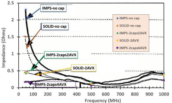 Figure 2a. Electrical performance of IMPS is very close to solid planes. A. Power distribution impedance versus frequency using HP8510 network analyzer.
 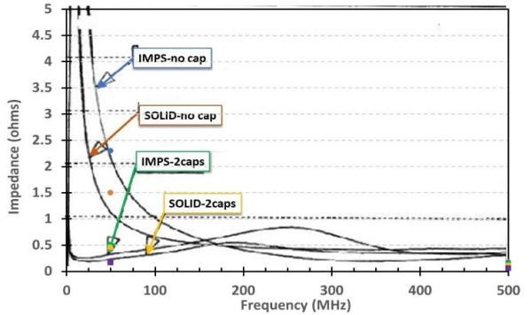 Figure 2b. Power distribution impedance using the HP4291A impedance meter.
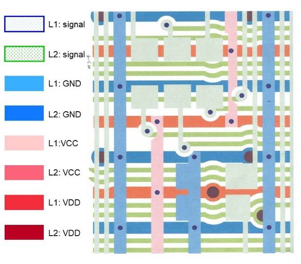
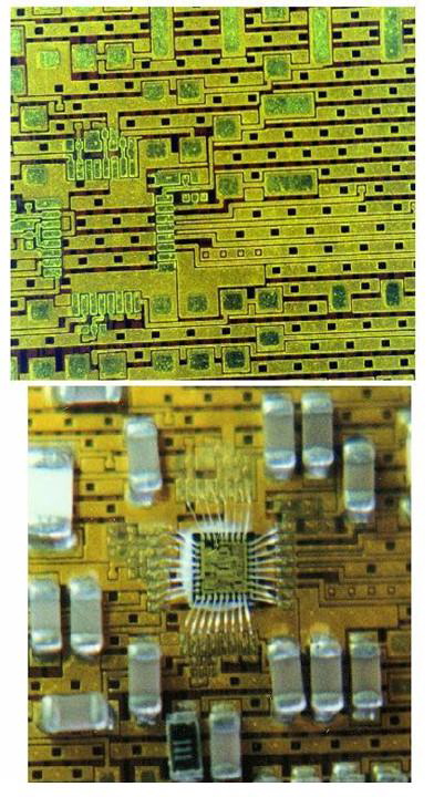 Figure 4. An IMPS topology before and after assembly.
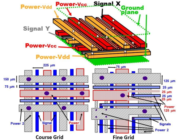 Figure 5. Power Mesh was adapted from the IMPS architecture but does not route GND bussing.
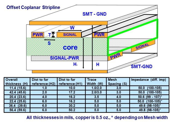 Figure 6. The impedance and crosstalk model for Power Mesh is an offset coplanar stripline. The table presents single-ended and differential impedances for various traces and thickness
 Figure 7. Example of a Power Mesh design. a. Innerlayer (L2 & L3) with buried vias b. Finished four- layer Power Mesh multilayer with microvia-in-pad and unbroken ground plane.
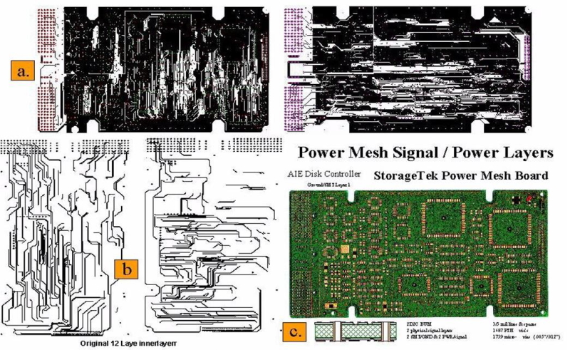 Figure 7. Example of a Power Mesh design. a. Innerlayer (L2 & L3) with buried vias b. Finished four- layer Power Mesh multilayer with microvia-in-pad and unbroken ground plane.

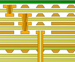
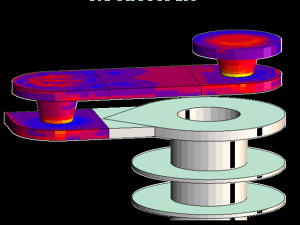
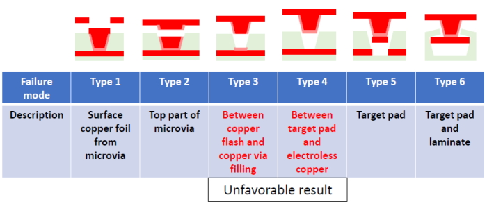
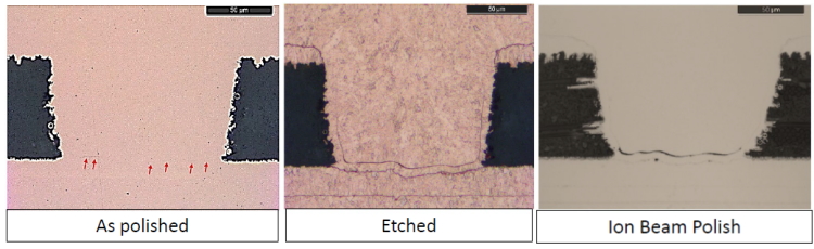 Figure 1: Cross-section of a microvia in as-polished condition (left), sharpened to show a hint of a crack between plating boundaries (red arrows); after microetch (middle) and after ion beam cleaning (right)
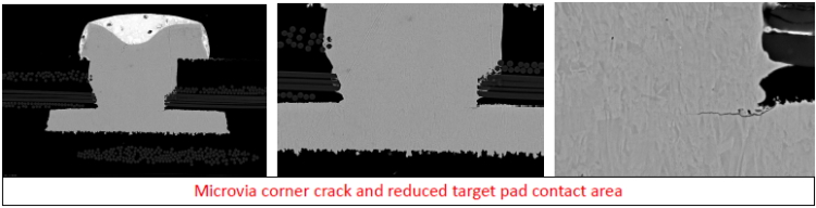
 The desmear process is critical. Inadequate adhesion between electroless copper and target pad is an important failure mode of microvias. A desmear cleaning process should be implemented to clean target pad (and hole walls) after laser drilling. Desmear may be performed using plasma. The efficiency of plasma desmear should be specifically verified across a panel, and from panel to panel depending on its position inside the chamber. Desmear should also be performed using wet chemistry (permanganate). A combination of both should typically be performed, in which case plasma should occur before wet chemistry, because wet chemistry can help removing remove ash residues from the plasma process.
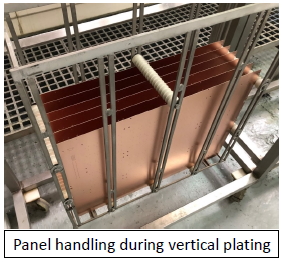
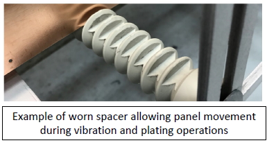 The efficiency of the desmear process should be verified across the panel, among panels of a job load (basket or rack) and among batches. Periodic, e.g., daily, weight loss measurement on test samples of applicable laminate types should be done to ensure process efficiency. To accurately measure the expected low amount of weight loss, it is essential to implement a strict measurement protocol, including bake out, elimination of static charge, environmental control of relative humidity and temperature. The protocol can be obtained from the chemistry supplier. The weight loss values should be determined taking into consideration the materials, technology and equipment set-up.
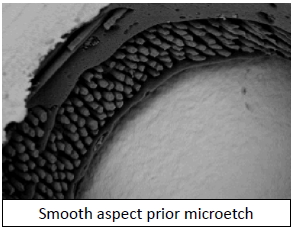 Persulfate may be used for microetch to remove film layers from the conditioning and activation processes (e.g. for plated through-hole manufacturing) and to increase the surface topography by exposing the copper grain structure. This will increase micro-roughness. Sodium persulfate or potassium peroxymonosulfate is recommended for its stable etch rate.
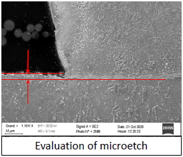
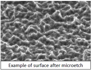 Etching efficiency inside microvias should be verified periodically across the panel and from panel to panel depending on its location in the bath. Longer process time at a lower etch rate typically provides better uniformity across the panel. Etching efficiency can be verified for instance by roughness measurement or penetration depth measurement using DPA and top-down SEM imaging. The copper roughness on target pad is the result of laser, pre-etch, desmear and microetch. Copper roughness on intermediate plated copper layers (e.g. flash copper) is the result of microetch only. Etch rate on the surface of a test sample should be verified prior to each working shift. The etch rate coupon should be used only once because the measured etch rate will change on a single, aged coupon. Procedures should specify if the coupon needs to be pre-cleaned and what possible effect such surface preparation may have on the etch rate measurement. Plated copper etches at a different rate than copper foil (that is typically of type ED electrodeposited). The correlation between the etch rate of a test sample and the etch rate of copper plating (that is on the surface of the target pad) should be established.
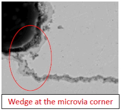
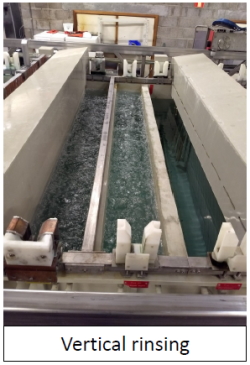 Rinse processes should be implemented in almost all main process steps. Each process step should have its own dedicated rinse. Cross contamination to other baths should be prevented by cascade rinse and/or counterflow rinse. Alternatively, a high rinse flow on a single bath may also be efficient. Efficiency of rinsing should be verified by investigating the dilution factor and cleanliness of the final rinse bath. Typical dilution factors are 2000 to 10000.
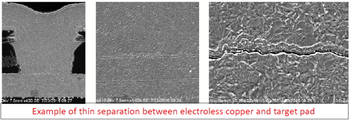 Deposition rate inside microvias should be correlated with deposition rate obtained on the test sample. This is named throwing power. This verification can be achieved, for instance, by overplanting with nickel (galvanic or electroless) to avoid smearing of copper (during microsectioning) and subsequent SEM analysis. The deposition rate should be verified using the test sample prior to each working shift. The sample laminate of the test sample should be used only once, because the measured plating rate on an aged sample will change. The sample should be of the same laminate as the technology to be manufactured and copper cladding should be etched off.
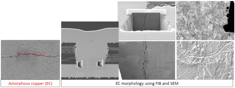
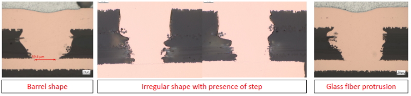
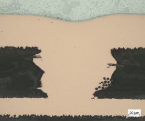
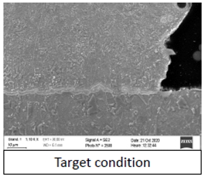
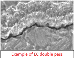 The electroless copper adhesion to target pad should be verified periodically, for instance by pull test or thermal stress and DPA. The morphology of electroless copper should be verified and compared to the target pad and plated copper. Aligned grain boundaries and visible interfaces are an indication of poor joint integrity. The aspect should not be amorphous. Top-down SEM inspection is preferred over cross-sectioning to avoid polishing artifacts and because it allows to inspect a larger surface area.
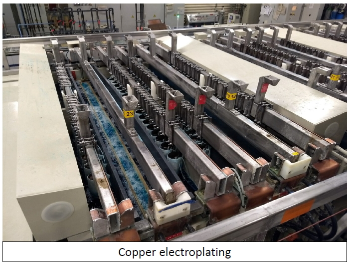 Waiting time in galvanic bath after the nominal duration of plating should be avoided. Zero current can result in reversed or unexpected plating and cause deposition of contaminants on the freshly plated copper layer. Care should be taken that residual low current does not result in different copper crystallographic structure. Maximum duration for residual low current should be specified and substantiated by characterization of the copper. Full current is recommended for microvia reliability, but it has the disadvantage of plating thick copper (on surface).
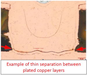
|
AGM and Technical Seminar March 2nd 2022 |
|
 ICT Chair ICT Chair |
A two-year project funded by an Innovate UK SMART Grant aims to reduce the impact of e-waste using naturally derived, biodegradable and nontoxic products. Those attending the webinar for the Institute of Circuit Technology’s annual meeting on March 2 learned more about the project, as well as statutory paperwork obligations as of the UK REACH regulations. Following the formal business, ICT Chair Emma Hudson introduced and moderated this technical webinar, which brought a final update on the progress of the ReCollect project and discussed the legislative implications of the UK REACH regulations. |
|
|
The ReCollect Project ReCollect (Efficient Manufacturing of Recyclable Composite Laminates for Electrical Goods) was a 30-month project funded by the Innovate UK SMART Grant scheme and led by Jiva Materials, partnered with Coventive Composites. The ReCollect project aims to reduce the impact of the e-waste stream using naturally derived products, biodegradable and non-toxic. Proposed as an alternative way of managing end-of-life circuit boards, the project is focused on removing glass fibre and epoxy resin from the supply chain by the use of a novel recyclable laminate technology known as "Soluboard," based on woven natural fibre reinforcement and a polymer soluble in hot water. At end-of-life, this material can be recycled simply by immersing it in near-boiling water, causing the polymer to dissolve, enabling the fibre reinforcement to be easily separated for reprocessing or composting, and the electronic components and circuitry to be recovered intact. The primary objective was to demonstrate the feasibility of producing a PCB substrate in high volumes with performance comparable with CEM-1 and FR-4 within the UK. The secondary objective was to ensure that this substrate was compatible with existing aqueous etching and plating processes used in PCB fabrication. ICT had provided dissemination and industry feedback. The project has now ended and Jack Herring, managing director of Jiva Materials, gave a meaningful summary of what had been achieved. Herring described the initial target market as commodity PCBs in domestic equipment, waste from which constituted 32% of WEEE. Products included PC peripherals, power circuits, and LED lighting. He reminded the audience that the WEEE directive placed the responsibility for waste recovery on the manufacturer of the product, and that Soluboard PCBs could be removed for recycling from products recovered through WEEE take-back schemes. Considering carbon savings, he stated that the carbon footprint of one square metre of Soluboard is equivalent to 7.1 kg of CO2, compared with 17.7 kg for a similar square metre of FR-4, representing a 60% reduction. And the plastic saving of Soluboard compared with FR-4 is 620 grams per square metre. A selling price equivalent to that of FR-4 can be achieved, and the material can be supplied in the form of a copper-clad laminate for PCB fabrication or an unclad laminate for printed electronics applications. It had been demonstrated that Soluboard is compatible with industry-standard wet processes for PCB fabrication. It is straightforwardly drilled and routed, and PCB assemblies can be successfully soldered with low-temperature alloys. Herring showed examples of boards for power supply units produced by print-and-etch technology, with thermally cured solder resist. A further example was boards for LED lighting, engineered to achieve the required reflectivity levels. In a printed electronics context, unclad Soluboard has been used to produce boards for Arduino microcontrollers using industry-standard functional silver inks. Preliminary technical data sheets had been prepared with a comprehensive listing of mechanical and electrical properties. The material has a flammability rating equivalent to UL94V-0, and is expected to be formally recognised shortly. Looking Ahead In terms of substrate development, the first version of Soluboard had a relatively coarse-weave jute-fabric reinforcement. A finer-weave fabric enabled improved electrical properties and would form the basis of a second-generation laminate. The solubility of the resin component clearly presented some obstacles to be overcome when aqueous plated through-hole chemistries were encountered, and this was a further area of development to be tackled once more funding was secured. Another topic of interest was in-mould electronics, where the thermoplastic properties of Soluboard make it an appropriate choice, and efficient recycling equipment to process Soluboard recovered from take-back schemes will be developed. |
|
|
A Systematic Approach to Regulations Continuing on a theme of chemical conscientiousness and the exciting world of legislation, we were reminded by Colin Martin, senior partner at ParaChem Consulting Chemists, of our statutory responsibilities under the REACH (registration, evaluation, authorisation and restriction of chemicals) regulations. REACH was formed in 2007 as a European chemicals’ regulation aimed at improving the protection of human health and the environment by identification of the intrinsic properties of chemical substances. The UK formally left the EU on 31 January 2020 (“BREXIT”), so the EU REACH regulations were no longer legally binding. They were replaced by UK REACH, a new statutory requirement to disclose information about the composition of manufactured “articles,” and disclosure requests would still travel up the supply chain from any EU companies. The UK government department responsible for REACH is the Department for Environment Food and Rural Affairs (DEFRA), which carried out a survey to establish the status of UK industry with regard to REACH compliance. It concluded that there was little understanding by manufacturers of REACH and its consequent obligations. Most of industry was not aware of the regulations or their implications, even though it was actually a criminal offence not to comply with disclosure duties. Having just published the results of their survey, DEFRA is now taking an active stance on REACH, and its regulations will be enforced. What happens next? Martin set out to disentangle the complexities of the procedures and present a systematic approach to compliance. He emphasised that, although this will involve a commitment of resources, it need not be overwhelming if the exercise is tackled methodically. It is necessary to compile a database providing data on “substances of very high concern,” (SVHC) in manufactured articles. The database will need to include inventories of all manufacturing consumables and all manufactured or bought-in items, with SVHCs identified and their mass percentages calculated. The minimum information required to provide to the consumer is the name of the SVHC, and this needs to be provided within 45 days. Specialist proprietary software is available to help in managing the database. Martin gave an example listing of all consumables and their compositions, and then looked specifically at the individual components of a particular product, with the composition of a fictitious proprietary solder mask used for illustration. The concentration of each of these consumables in the product was determined. Similarly, his inventory of articles listed all the ingredients used in the manufacture of each article and their mass percentages. Once all of this data-gathering had been completed, it provided a resource from which five categories of formal report could be prepared: UK SVHCs at concentrations greater than 0.1% contained in individual articles, similar for EU SVHCs, customer reports of UK SVHCs contained in articles, similar for EU SVHCs, and a European Chemicals Agency report if more than 1,000 Kg of any SVHC was being processed in a year. As one who had enjoyed a career coming to terms with the technicalities of actually manufacturing printed circuit boards, I was reminded that today’s statutory paperwork obligations extend far beyond routine production and quality assurance documentation. Pete Starkey |
 Chief Product Officer,
 Senior Partner,
ICT Winter Seminar Review: Nov 2021
|
|
 Technical Editor, Technical Editor,iconnect007 |
Faced with the choice between a real or virtual event, Bill Wilkie took a calculated risk. It has been many long months since members of the Institute of Circuit Technology had gathered together under one roof, but a fair-sized bunch of industry stalwarts braved the weather and the threat of COVID, descended on the Manor Hotel in Meriden, UK, on November 30, and applauded Bill’s decision to go live. They were not disappointed; the program was superb, the atmosphere upbeat, and the networking opportunity priceless. |
|
Nikon Metrology |
Advances in X-ray MetrologyThe first presentation came from Richard Frisk, sales account manager with Nikon Metrology, who gave a fascinating introduction to recent advances in X-ray inspection systems, particularly regarding their applications in solder joint inspection but with many examples of their ability to examine the finest details in all kinds of electronic and mechanical structures. Frisk briefly introduced the company, which had three other specialist divisions: imaging products, semiconductor lithography systems, and healthcare, in addition to their interests in industrial metrology. He commented that the Nikon name derived from “Optics from Japan.” Although X-ray imaging systems had been used for many years as an aid to PCB manufacturing, their main historic application had been for checking registration in multilayer boards. There had been many advances in capability over the last 20 years and Frisk described three types of X-ray image that had particular uses in solder joint inspection: radiography, computed tomography and laminography. He emphasised that, for metrology, good image quality was the basis for accurate measurements. Using radiographs of a soldered BGA device, he demonstrated how radiography was used to detect and measure voids in the solder joints, explaining that it had become normal practice to invert the image so that the denser the material the darker it would appear and voids would show as light within a dark background. A view with the X-ray source and detector normal to the PCB showed clearly defined solder balls and bond wires. Some solder balls showed evidence of voids and it was possible to calculate the percentage of solder ball area to void area and apply accept-reject criteria to the images. An oblique view gave the effect of seeing the image in perspective and enabled voids to be further classified as “near to the PCB-solder interface,” “near to the IC-solder interface” or “mid-ball,” and features like poorly formed solder joints and head-in-pillow type defects could be identified. Resolution was high enough to enable wire-bond and die attach inspection, and the examination of individual balls. Typical X-ray settings were 110 kilovolts and 130 microamps. He showed several analysis examples and inspection algorithms for BGA devices, although he commented that radiographs could get very “busy” and needed a skilled operator to make judgements. Computed tomography was a scanning process whereby the sample was continuously rotated whilst thousands of X-ray images were taken and then reconstructed by a powerful computer into a three-dimensional volume from which two-dimensional slices could be sectioned in any direction and a three-dimensional model generated, enabling in-depth automated defect analysis and measurement at high resolution. Individual materials could be colour-coded and Frisk’s examples of the structure of QFP and BGA components were spectacular in their detail. With flat samples such as PCB assemblies, a limitation of computed tomography was the distance that could be fully penetrated as the sample was rotated parallel to the X-ray beam. In comparison, laminography was a non-destructive inspection technique for samples of any size that enabled the virtual micro-sectioning and analysis of large boards with typical scan times of less than five minutes. Laminography could be used to view defects in multi-layer PCB assemblies and devices and for early identification of latent defects. Frisk held the audience spellbound with some video examples of fault-finding and forensic applications which demonstrated the capability and versatility of currently available X-ray equipment. |
|
CEO, |
A Solution for E-Waste?“The world’s first recyclable PCBs” were features of the presentation by Dr. Jonathan Swanston, CEO of Jiva Materials, originators of the Soluboard recyclable PCB substrate. Swanston began with the frightening statistic that 54 million tons of waste electronics and electrical equipment are produced world-wide annually, and the quantity continues to grow. His figures indicated the UK alone to be responsible for generating the equivalent of 23.9 kilograms per person, a total of 727,000 tons, and that 32% of all e-waste consisted of small domestic equipment. Against that background, he described the characteristics of Soluboard, a composite laminate based on natural materials bound by a non-toxic and biodegradable resin soluble in hot water, with physical properties comparable to those of market leaders. The carbon footprint of one square metre of Soluboard was equivalent to 7.1 kg of carbon dioxide, compared with 17.7 kg for one square metre of standard FR-4, indicating a 60% reduction in carbon footprint and a saving equivalent to 620g of plastic per square metre compared with FR-4. Swanston described two versions of his material, a copper-clad laminate for subtractive processing, with woven fibre reinforcement based on jute, and a bare laminate for printed electronics with woven fibre reinforcement based on flax. The manufacturing sequence for the unclad version followed similar impregnation, drying, layup and press lamination stages to those used in conventional laminate production. Copper foil could be subsequently press-bonded to unclad material using an adhesive. The process stages for producing PCBs were basically similar to standard practice. Conductive silver ink was used for assembly of printed electronics substrates and low-temperature solder for etched circuits. He showed an example of a fully assembled prototype single-sided Arduino board produced by Jiva Materials. It was believed that the mechanical and electrical properties of Soluboard would meet the requirements of most sectors within the electronics industry. Testing to IPC standards was in progress and expected to be completed shortly, with UL recognition to follow during 2022. Jiva’s initial target market was a share of the 2.8 billion square metres of FR-4 currently used in single and double-sided boards for domestic appliances. |
|
Senior Research Scientist, |
Electronics Research ProjectsAlthough gaining access to the third presentation may have tested Bill Wilkie’s IT skills, his efforts were rewarded when the connection was successfully made and a virtual presentation was received online from Martin Wickham, senior research scientist at the National Physical Laboratory. It was clear that there was a lot going on at NPL. Wickham gave an update on a busy program of new electronics research projects meeting current challenges in electronics reliability. Smaller, lighter, faster, cleaner, smarter, hotter—these were the inevitable buzzwords, reducing CO2 emissions toward “net zero” was a major driver and there was general push toward higher voltages. One of the main projects in the 2021-2022 program was the continuing study of high voltage “partial discharge” effects, which could occur as a “spark” in the insulation between two conductors at a point where the electric field exceeded the local dielectric breakdown strength and was often associated with minor defects in the dielectric. Partial discharge could occur multiple times at lower voltages and progressively reduce the breakdown strength of the insulation. A multi-channel test system had been developed and used for an initial evaluation of partial discharge and insulation resistance at high voltage. The system could operate at voltages up to 10,000V. Work to date had concentrated on twisted pairs representing motor insulation but would shortly be extended to include PCBs. The second phase of the ongoing study of conductive anodic filament (CAF) effects at high voltages had recently been completed. Test boards with different design details for CAF and surface insulation resistance (SIR) monitoring had been aged at 1000V DC, with hole-to-hole distances in the range 550 to 2100 microns for CAF and pad-to-pad distances of 440 to 1950 microns for SIR. All the CAF patterns had failed within 2,000 hours but there had been no SIR failures for the three no-clean solder pastes tested. The time to failure for CAF was inversely related to DC voltage. NPL had proposed a multi-partner project for investigating CAF failure, and IPC had organised a round robin on the prevention of SIR failures in CAF testing. Electrochemical impedance spectroscopy had been utilised for rapid materials evaluation. This used AC impedance to determine the impact of flux residues, as an alternative to traditional DC SIR measurement. It was expected that its predictive capability could be developed into a non-destructive test method. Wickham also briefly discussed developments in fast turnaround insulation resistance testing in damp environments, platen condensation testing, immersion testing and rapid in-process conformal coating evaluation, as well as a new measurement facility and test vehicles for the quick assessment of reliability of coatings under harsh conditions. Industry collaborators were invited to join a multi-partner project to evaluate electronic materials for harsh environments. |
|
CEO, |
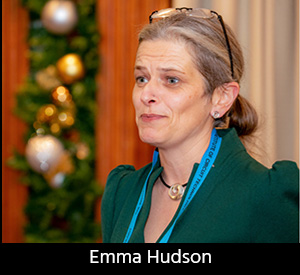
Solder LimitsThe final presentation, forewarning the industry of imminent changes in UL solder limits, came from ICT Chair Emma Hudson. Urging material suppliers and PCB fabricators to get prepared without delay, she explained that solder limits were key parameters for UL Recognized PCBs, representing the soldering processes to which the PCB would be exposed during assembly operations and capturing all time spent over the maximum operating temperature and the maximum temperature reached. They were employed in many of the test procedures used to characterise a PCB as part of the recognition process. Hudson stressed that if solder limits were exceeded during PCB assembly, the safety evaluation conducted on that PCB was invalidated. Reviewing current status, she explained that the new editions of standards UL 796 for printed wiring boards, UL 796F for flexible circuits, UL 746E for laminates and coatings, and UL 746F for flexible materials, recently published, had all included standardised solder limits and assembly solder process requirements. These defined all the time spent over the maximum operating temperature, or 100°C whichever was greater, and the maximum temperature reached as measured on the surface of the PCB. The standards now included a new default solder process condition: six cycles of the IPC T260 profile. UL had issued a bulletin to all manufacturers with PCBs Recognized under UL 796 and UL 796F explaining the concept of standardised reflow profiles, the updates to the standards and how they would be implemented. UL Follow-Up Services would verify at the assembly company that any board certified from January 1, 2022 had suitable solder limits and assembly solder process parameters for the actual process, and if any PCB was not Recognized with the appropriate parameter it would be deemed a non-conformance. Any changes or modifications to existing PCB types, including the addition of new materials, conductor parameters, solder limits, maximum operating temperatures and flammability rating made from January 1, 2022 would also be subject to the new inspection criteria. Existing board types that remained unchanged could be left as they were. Hudson highlighted the need for laminate and solder resist manufactures to update their materials to the new solder limits and assembly solder process parameters, preferably to the default of six cycles of the T260 profile, otherwise the PCB manufacturers would face much more testing. She advised PCB manufacturers to talk to their laminate suppliers without delay about their plans to upgrade their material Recognition. Some testing would still be needed to upgrade PCBs to the new assembly solder process solder limits but if materials had the new values the amount of testing could be reduced. Similarly, solder resist suppliers could adopt the default assembly solder process parameters and their associated flammability testing requirements. She suggested that PCB manufacturers who had impending changes to existing PCB types should consider the creation of duplicate types in their UL files, making copies that could then be updated as and when necessary, depending on the ease of maintaining the PCB type designation with their customer. Her closing words were: “Be prepared as a PCB manufacturer. This is happening. Ask your material suppliers what they are doing to help you.” |
|
The Institute of Circuit Technology Autumn Seminar 2021 was a great success. It provided an excellent technical programme and much more. It was a gathering of real people and a long-awaited networking opportunity. |
|
| Go back to Contents |
|
Bill Wilkie |
Directors ReportBill Wilkie, ICT We are holding our Annual Foundation Course as a live event this year at Chester University with the first day at Merlin pcb, Deeside to be able to enjoy a facility tour in the afternoon. The Halls of Residence are not available this year, due to covid restrictions, so we have arranged accommodation at a local hotel, within easy reach of the campus. Read more.... Our Annual Symposium will also be live at the National Motor Museum at Gaydon with Happy Holden delivering the Keynote. Read more....
|
Industry News |
|
| Parachem |
We recently received a communication from DEFRA via the HSE regarding downstream user duties under UK REACH. It is very relevant for ICT member companies. Important news regarding "Reach" Article 33 – Duty to disclose information about SVHC conatained in manufactured items. The Department for Environment, Food and Rural Affairs (DEFRA) has launched a survey via the HSE e-Bulletin service in order to: SPECIAL OFFER FOR NEW SUBSCRIBERS TO REACHWARE® It also facilitates compliance with; EU REACH Reporting Duties What’s the deal? Any ICT corporate or individual member can subscribe to ReachWARE® for a reduced monthly fee. The subscription is normally £60+VAT per month, and this will be reduced to £45+VAT per month for twelve months for ICT members taking out a subscription in April 2022. Furthermore the £199+VAT set-up fee will be waived throughout April 2022. There is no tie-in period and you can terminate your subscription at any time. How do I sign up? You can see information about ReachWARE® on our website before subscribing. There are downloadable guides to help with all aspects of using ReachWARE®. Go to our website parachem.co.uk and register your interest. All enquiries received on or before 30th April 2022 will qualify for the discounts described above. |
| Atotech | Atotech took part in IPC APEX EXPO 2022 and presented four technical papers this year, touching on the following hot industry topics “crystal structures in plated microvias”, “electroless palladium plating”, “Pd-free activation for electroless Cu”, and “nano structuring photoresist adhesion promoter”. Read more.... |
| CCI Eurolam | Christian Winkler – New colleague in Technical Sales CCI is growing and our sales department is being further expanded. We are pleased to announce that Christian Winkler will be supporting us with his knowledge and experience as of 1 February 2022. Read more.... |
| Eurotech |
Lyncolec Rebranded as Special Products Division of Eurotech. |
| Merlin Circuit Technology | Merlin Circuit Technology goes fully digital. The printed circuit board industry has always relied on photographic and mechanical disciplines in the manufacturing processes to derive circuit images, solder mask apertures and legend notations for the components. Expensive photo plotting machines have been produced with high-definition films to create super accurate photo tools, however, this process carries… Read more |
| Merlin Flex |
Merlin Flex, a global supplier of Flex & Flex/Rigid interconnect solutions, has been on the SC21 journey for over 10 years and after several years of continuously achieving the Bronze award, the company is pleased to announce it has achieved the Silver award status. Read more.... |
| Teledyne Labtech | Teledyne Labtech Announces New Advanced Graphite Embedding Capability for PCB Thermal Management. New innovation provides weight savings for applications where size, weight and power (SWaP) are key. - Teledyne Labtech announces a major new capability allowing the embedding of layers of synthetic graphite within RF and microwave printed circuit boards (PCBs). Heat management is a significant concern in many aerospace defense and space applications where size, weight and power (SWaP) are key attributes. Gallium nitride (GaN) solid state power amplifiers (SSPAs) are examples of increasingly common devices that benefit from careful heat management. This new technique allows efficient conduction of heat away from such devices, saving system weight and increasing their lifetime. Read more.... |
| Ventec | Ventec announced that the asset purchase agreement with Holders Technology (AIM: HDT) in Europe was completed on October 21, 2021. The transaction completes Ventec’s acquisition of a range of PCB assets owned by Holders Technology’s German & UK operating subsidiaries. Read more.... |
| Zot |
Zot Printed Circuits are pleased to announce that they have placed an order for a new Schmoll MDI - supplied and installed by Schmoll Maschinen GmbH. The new digital imaging system increases capability and capacity for processing high technology, high reliability Printed Circuits. Read more.... |
| Go back to Contents |
Membership News |
||||
|
Bill Wilkie |
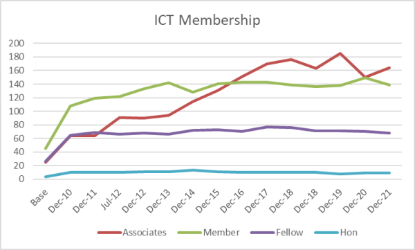 There are currently 382 members of The ICT spread across the categories shown in the chart There are currently 382 members of The ICT spread across the categories shown in the chart |
|||
|
|
NEW MEMBERS SUMMARY October 2021- March 2022 |
|||
| Membership No | Name | Company | ||
| Hon Fellows - The following past chairs of the Institute have been awarded Honorary Fellowship in recognition of their exceptional contribution to The ICT. | ||||
| 583 | Steve Payne | iNEMA | ||
| 1036 | Chris Wall | Electra | ||
| 2002 | Martin Goosey | MTG Research | ||
| 10026 | Andy Cobley | Coventry University | ||
| Fellows | ||||
| 10551 | Gordon Falconer | Zot Engineering | ||
| Members | ||||
| 10552 | Janine Schwestka | RUAG Space | ||
| Associates | ||||
| 10553 | Jeff Cox | C-T Machinery | ||
| Reinstatement | ||||
| 10022 - Fellow | Chris Hunt | Gen3 Systems | ||
| 10172 - Fellow | Steve Driver | Jiva Materials | ||
| Go back to Contents | ||||
Corporate Members of the ICT |
||
| Adeon Technologies BV | www.adeon.nl | |
| Amphenol Invotec Ltd | amphenol-invotec.com | |
| Atotech UK Ltd. | www.atotech.com | |
| CCE Europe | www.ccee.co.uk | |
| CCI Eurolam | www.ccieurolam.com/en/ | |
| Electra Polymers Ltd | www.electrapolymers.com | |
| The Eurotech Group | www.eurotech-group.co.uk | |
| Exception PCB Solutions | www.exceptionpcb.com/ | |
| Faraday Printed Circuits Ltd | www.faraday-circuits.co.uk |
|
| Flexible Technology Ltd | www.flexibletechnology.com/ | |
| Graphic plc | www.graphic.plc.uk | |
| GSPK (TCL Group) | www.gspkcircuits.ltd.uk | |
| HMGCC | www.hmgcc.gov.uk | |
| Holders Technology UK | ww2.holderstechnology.com | |
| Merlin Circuit Technology Ltd | www.merlinpcbgroup.com | |
| Merlin Flex Ltd | www.merlinpcbgroup.com | |
| Minnitron Ltd | www.minnitron.co.uk | |
| Newbury Electronics Ltd | www.newburyelectronics.co.uk | |
| Photomechanical Services | www.creekviewelectronics.co.uk | |
| PMD | www.pmdchemicals | |
| Stevenage Circuits Ltd | www.stevenagecircuits.co.uk | |
| Teledyne Labtech | www.teledynelabtech.com | |
| Trackwise Designs Ltd | www.trackwise.co.uk | |
| Ventec Europe | www.ventec-europe.com | |
| Zot Engineering Ltd | www.zot.co.uk | |
| Go back to Contents |
ICT Council Members |
|
|
Council Members |
Emma Hudson (Chair), Andy Cobley (Past Chairman), Steve Payne (Hon Deputy Chairman), Chris Wall (Treasurer), William Wilkie (Technical Director, Hon Sec, Membership & Events), Richard Wood-Roe (Web Site), Lynn Houghton (Hon Editor), Jim Francey, Martin Goosey, Lawson Lightfoot, Peter Starkey, Francesca Stern and Bob Willis, |
Editors NotesThe ICT Journal |
|
|
Lynn Houghton |
Instructions / Hints for Contributors 1. As it is a digital format the length is not an issue. Short is better than none at all! 2. Article can be a paper or a text version of a seminar or company presentation. Please include data tables, graphs, or powerpoint slides. We can shrink them down to about quarter of a page. Obviously not just bullet points to speak from. 3. Photo's are welcome. 4. We would not need source cross references 5. Title of presentation - Of course! Date, Job title of Author and Company represented. 6. An introductory summary of about 150 words would give the reader a flavour of what it's all about. 7. Style - we don't want out and out advertising but we do recognise that the author has a specialism in the product or process that will include some trade promotion. Sometimes it will be a unique process or equipment so trade specific must be allowed. 8. Date and any info relating to where or if this article may have been published before. 9. We can accept virtually any format. Word, Powerpoint, publisher, PDF or Open Office equivalents. 10. Also, to make it easy, the author can provide a word file to go along with his original powerpoint presentation and I/we can merge it together and select the required images. 11. A photo of author or collaborators.
I really do look forward to receiving articles for publication. Lynn Houghton |