

The Journal of the Institute of Circuit Technology Vol 11 No 2 May 2018 |
|
| Links to Contents | Section |
| Calendar of Events | 1 |
| 2 | |
| Council Members | 3 |
| 4 | |
|
ICT Evening Seminar and AGM at Meriden, Solihull. March 13th 2018 |
5 |
| 6 | |
| 7 | |
| 8 | |
| 9 | |
| 10 | |
| Corporate Members 11 | 11 |
| Publishers Notes 12 | 12 |
| Section 2 | It's As Good As We Get |
|
Editorial |
Bruce Routledge has done a fantastic innovative job in creating the ICT Journal and editing it for the past 10 years. Perhaps it would be impolite to mention his age but unfortunately the time has come for him to shut down his laptop and pass on the responsibility of the Journal to others. We really want the Journal to continue and flourish. Regular readers will know that Bruce was always asking for papers and articles to include in the Journal. We want to expand the scope of the Journal to make it a source of news, updates and information about our individual members, our corporate members and the PCB industry, as well as being the Technical Journal of our Institute. We can't create something from nothing so it really is “As Good As We Get”. At the moment I have volunteered to act as publisher. That means collating material that is submitted and preparing it into a format that will be distributed to members on a regular basis. We currently have 400+ individual members at all levels of experience and expertise, mainly UK based with a significant number of overseas members. We have 18 corporate members who represent the complete breadth of PCB manufacturers, equipment providers and chemical suppliers. If you have something that you believe may be of interest to our members then please let me know. If you have company news then shout about it here. If you have an innovative process or equipment development then our members will want to know about it. If you have a research or development project then report the results and involve our members here. Don't forget that there are no charges for items published. There are no adverts and no hidden fees! We can accept virtually any form of input such as presentation files with notes, photos, text, word documents and publisher files. Please see some guidelines at the end of the journal - Link to guidelines I look forward to the next phase of our Journal with keen anticipation. Richard Wood-Roe |


| Section 6 |
Metallisation of Textiles to make Urban living for Older people more Independent and Fashionable The MATUROLIFE Project. |
|
Professor Andy Cobley, leader of the Functional Materials Research Group at Coventry University and ICT Chairman |
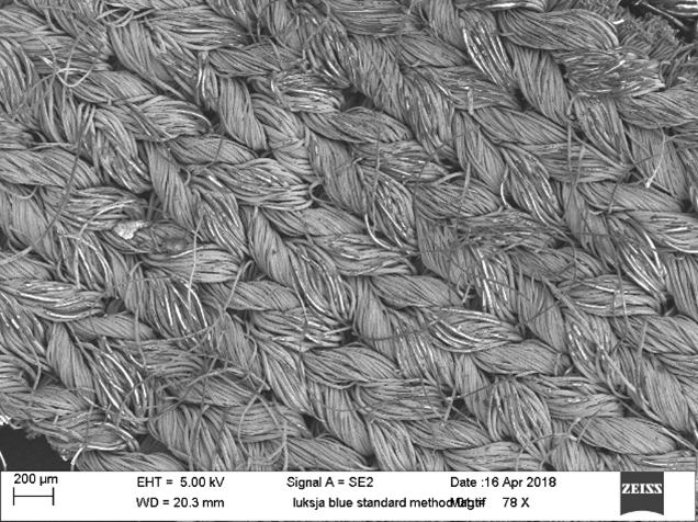
Authors – Prof Andrew Cobley, Dr Daryl Fox, Dr Golnaz Taghavi Pourian Azar The Functional Materials Group, Coventry University, UK Electronic or ‘smart’ textiles represent a potentially high growth area for electronics manufacturing. There are a number of ways to make textiles and fabrics conductive including knitting or weaving in conductive threads or metal wires or printing conductive inks onto such materials. However, these approaches have their drawbacks. In addition, in many cases, it is arguable whether such approach can produce electronics that are truly integrated into the textile as conventional metal wires change the feel and drape of the material and make them stiff and less flexible. Simply attaching electronic components to a textile makes them heavier and uncomfortable to wear. The MATUROLIFE (Metallisation of Textiles to make Urban living for Older people more Independent and Fashionable) project led by Coventry University (UK), which is funded by the European Commission and involves 20 partners from 9 countries, takes an alternative approach to introducing connectivity to textiles and fabrics. Building on collaborative work carried out between Coventry University and the National Physical Laboratory, the project will use processes common in PCB manufacture to produce conductive ‘smart’ textiles. In MATUROLIFE, catalysts will be developed that can be selectively deposited onto textiles and fabrics enabling subsequent electroless plating processes to fully coat fibres within the textiles. Previous work has shown that only a relatively thin coating of electroless copper is required to produce highly conductive textiles. By coating the fibres in the textile with copper, a truly multi-functional material can be produced. The feel and drape of the textile is maintained with very little increase in weight whilst the material can still be bent and twisted in the same way as a conventional textile. Early results from the project have shown that a conventional electroless copper plating process typically used in PCB manufacture (Conditioner, pre-dip, Catalyst, Electroless Copper) can be used to successfully metallise a variety of textiles and fabrics. Figure 1 shows an SEM of a polyester material with a uniform coating of electroless copper.
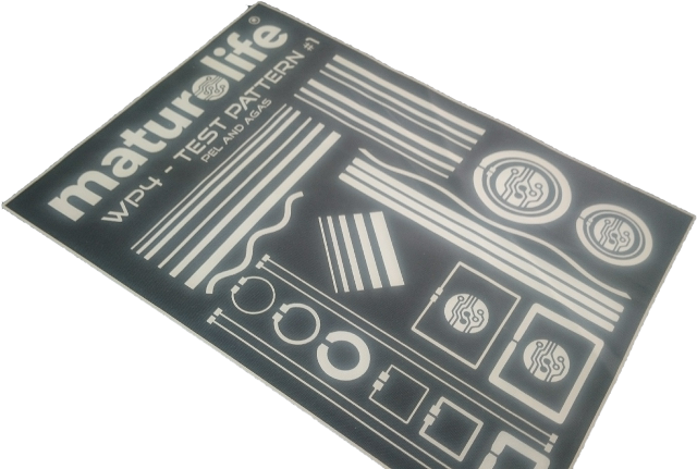
Figure 1. Scanning Electron Microscope (SEM) image of polyester material coated in Electroless Copper using electroless copper process chemistry supplied by AGAS Electronic Materials Ltd Methods will be developed to selectively deposit catalysts that will initiate electroless copper plating. In this way circuits and electronic connectivity can be introduced to textiles and fabrics. A MATUROLIFE test pattern has been developed by project partner Printed Electronics Ltd and is shown in Figure 2 below.
Figure 2. The MATUROLIFE Test pattern printed by Printed Electronics Ltd. The MATUROLIFE project aims to use this approach to produce ‘smart’ textiles that can be used for Assistive Technology (AT) for older people. With an increase in the ageing population across Europe there is a huge and growing demand for AT. However, such devices are not designed with fashion, aesthetics or discretion in mind and are often obvious marking the person out as vulnerable and ‘older’. Obtaining the opinions and desires of older people will therefore be central to MATUROLIFE. The project will utilise a design management approach embedding creative artists and designers and their methods throughout the project. Product development will ensure embedding of emotional design principles and adoption of a co-creation approach. Thus, older people will influence the design of AT ensuring it is functional, meets their needs and requirements and is aesthetically pleasing and desirable. The MATUROLIFE project brings a unique multi-disciplinary approach to research in that it will bring together electrochemists, materials scientists and experts in electronic manufacturing processes with creative and artistic designers to produce smart textiles and fabrics that could revolutionise AT for older people, enabling the production of more discreet, and aesthetically pleasing AT with improved functionality making their lives easier and more secure. More, and regularly updated, information on the project can be found at our website maturolife.eu. You can also follow us on Twitter @maturolife. The author would like to thank the European Commission for funding this project (Grant Agreement No 760789) and our partners: AGAS Electronic Materials Ltd, Printed Electronic Materials Ltd, Eurocarers, CTCR, UPH – Siedlce, Pitillos, Luksja, IFTH, ITAINNOVA, Bertin Aubert Industries, Muebleconfort SL, Emo Design, Plasmachem GmbH, Univerza V Mariboru, ISN DOO, Age Platform Europe, GEDS, IPM2, Sensing Tex SL.
|

| Section 8 |
Printed, Conformal and Flexible Electronics Neil Chilton PhD Technical Director – PEL |
|
Dr Neil Chilton, Technical Director of Printed Electronics Ltd (PEL) |
It is now more than 10 years since Printable Electronics (PE) moved from academic research activity and into a commercially-viable, but often development-scale, form and in many areas a transition to high volume commercial-production has not yet been fully made. But both the real potential and the expectation remain high: incorporating PE components and systems can revolutionise product design and function. Over the last few years the manufacturing equipment, material portfolio and production capability available within the Printed Electronic and Large Area Electronics community has improved greatly. But at the same time, it must be remembered that conventional subtractive and lithographically-formed electronics offers an exceptional wealth of capability and resource. For example, PCB interconnection density will remain in advance of the production capability of most printable interconnects for many years to come. Therefore, it is essential to understand that printable electronics is not a competitive industry to PCB or conventional electronics and is better understood when seen as running in parallel with conventional manufacturing – and each can embrace the other to best achieve potential gains. In this article I will focus on activities in PEL and the wider community concentrating on areas where conventional PCB would be harder to implement – specifically looking at directly-printed, flexible and conformal electronics. I will outline current capabilities and highlight areas where the field has the potential to gain most commercial success. This article is based on a presentation given at the EIPC winter conference (Lyon 2018) and the ICT seminar (Coventry, 2018). About PEL Printed Electronics Limited (PEL) is a UK based manufacturer sited at the Amphenol Invotec facility in Tamworth UK, and with a sister site in Cambridge. The business is manufacturing-based with a core focus on process and product development involving printing and electronics (not always solely printed-electronics); specialist-equipment and materials sales; bespoke ink formulation and industrial scale up. PEL has been operating for more than 12 years and has a team of experts with a deep understanding of both electronics and printing technologies. In recent years a significant focus has been placed on combining Printed Electronics (PE) with Additive Manufacturing (AM) processes. PEL is also a member of the EU Graphene Flagship (https://graphene-flagship.eu/project/Pages/Consortium.aspx ) programme and is working with 2D materials in areas of both electronic and structural enhancement. We are often asked to develop and produce low to mid-volume specialist or “unconventional” circuitry and interconnects on a fast-turn. These are systems where the form and function of the part dictates that a PCB alone would not be appropriate, and often these printed elements have a lower level of complexity than a PCB; two or three layers of connection is common, but few printed solutions would be practical with more than, say, 6 layers, this is because yields significantly drop when adding further layers. The reason for this is that printed dielectric layers are often, for reasons including pin-holes, less capable than their equivalent in the conventional manufacturing world. Recognising that printing alone can limit functional capability means that we regularly make use of hybrid electronics: coupling conventional components with Printable Electronics. What’s in a name? With the name and domain of Printed Electronics we are in a fortunate position that we are found quite easily on web searches. However, there may still be some confusion over names used within this sector. Together with PE, the names Organic Electronics, Plastic Electronics and Large Area Electronics are all used. Essentially these are all aliases for this branch of electronics. The name organic electronics is perhaps used less widely now, partly because it is not straightforward to manufacture n-type semiconductors with solely organic materials and both p and n type are essential for CMOS structures. The name Large Area Electronics (http://www-large-area-electronics.eng.cam.ac.uk/what-is-large-area-electronics/) is possibly the most relevant in this field because the differentiator here is not so much the type of material used (organic, inorganic etc), nor is the method of application (printed or otherwise), instead it is the fact that this branch of electronics is one where the form factor is distinct from the panel-based approaches of “conventional manufacturing” in PCB, semiconductor or PV. The important ability is often to be able to manufacture in large format (even if the final part is smaller).
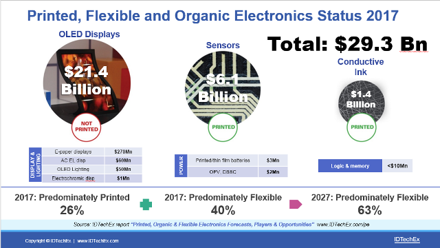
Figure 1 Forecast for Printed, Flexible and Organic electronics. Courtesy of IDTechEx (www.IDTechEx.com) What is the market? In the PCB industry the market size is known to a high level of accuracy thanks to the well-established works of Dr Nakahara, Walt Custer and others in this area – and all numbers are verifiable through import and export tax coding records etc. The true market size for Printed, Flexible and Large Area electronics though is subject to a little more interpretation. For this article we have been given the kind permission of industry specialists IDTechEx to use some of their analysis. IDTechEx report (Figure 1) that the available market for this sector is as high as $29bn. However, it is important to note, as IDTechEx also do, that this headline number includes OLED mobile phone screens (which are made almost solely using semicon fab methods), diabetes test strips (which are true printed electronics but are not new since they have been made using roll to roll printing for many years now) and the sales of conductive ink (which in addition to glucose test strips is used extensively in the manufacture of screen-printed capacitive touch interconnects on glass). But even excluding the headline revenue elements noted above that still leaves a market that is in the billion-dollar range. |
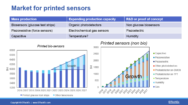
Figure 2 IDTechEx forecast for Printed Sensors, an area where there is widespread agreement that growth is occuring Now, to look for where the growth is expected to occur. Figure 2 shows the expected growth of medical and non-bio sensors over the coming years. Printed sensors open up a market that currently doesn’t exist. An analogy that could be used is that of smoke detectors in the home. 40 years ago, they were expensive and therefore rarely used in the home; now they are ubiquitous. Low cost sensors for pollutant and other gases will allow a similar growth to occur especially in industrial and medical monitoring use. But gas sensing is only one area where printed sensors are likely to be used. Another growth area is expected to be adding sensors to parts that currently have none – for example adding touch sensitivity to the surface of industrial robots or adding sensing capability to prosthetics. Here it is the form factor rather than the manufacturing method that is differentiating the devices. On the topic of form factor, this is – in PEL’s view – the most important differentiator to understanding where this market will head. Simply put, if you can adequately integrate your electronics using either rigid, flex or flex-rigid PCB then it is unlikely that you need to look outside of conventional electronics. However, if the form factor is somehow compromised by the fixed shape of the underlying PCB (inside its case) then this is where PE approaches can bring major benefit. |
|
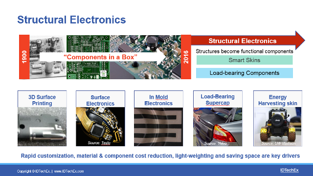 Figure 3 Structural Electronic – just one area where form- factor is demanding a change to the physical structure of the electronics used |
|
|
So, you have an interest…? Assuming then that the ability to create interconnects or electronic sensors in some sort of unconventional format is useful for your product, the next step is to consider how to go about forming these. It is also worth noting here that PEL works mainly in interconnects -and does not currently have a core capability in directly printed semiconductor, PV or gas sensors, so we will not cover that aspect of printed electronics in this article. One area of interest to PEL and partners is aerospace where lightweight circuits can provide significant commercial benefit. In aerospace SWaP (Size, Weight and Power) is a widely used acronym for critical design considerations. Enhancing any of these elements makes a material difference to performance. Some areas of interest that our aerospace partners have shown are in directly-printed interconnect structures, long and lightweight cable replacements, sensors and embedded circuitry also together with some wearable applications. |
|
|
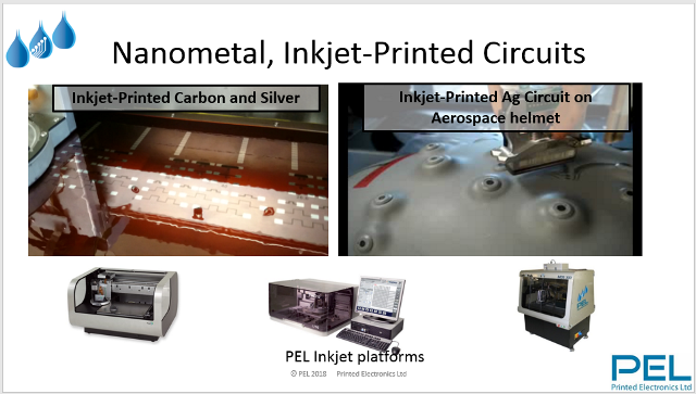
Figure 4 Inkjet printing of circuits Figure 4 shows two examples of directly (inkjet) printed circuit structures - one flat and one curved. The helmet application was done for light-weighting reasons: removing the weight of the circuit board itself brings a significant potential functional improvement. If you are now thinking “well, how heavy can a flex PCB be?” I need to add one more comment – this helmet is designed to be used by fighter pilots at up to 9G hence every gram matters up to nine times more. Inkjet-printed circuits based on metal inks can be directly printed onto a pre-existing surface so potentially eliminating the substrate and its weight. It is digital, additive and direct and gives the benefits of Additive Manufacturing. However, such circuitry is usually thinner, more resistive and more fragile than conventional electronics and it cannot generally carry significant current, so inkjet circuits are more applicable to sensors than power circuitry. To answer why the printed traces are |
|
|
thinner than conventional traces you need to consider the material that is actually printed by an inkjet head. All inkjet heads – whether it be the one sitting on the home/office desk or one printing gold sensors for medical applications – print a fluid ink[1]. The ink needs to have a low viscosity in order to be ejected from the head. The viscosity is slightly dependent on the head type but is around that of semi-skimmed milk – so not particularly viscous at all. For a metal-bearing ink, albeit with nano-particles of metal, the only way to achieve such a low viscosity is to have an ink where most of volume of the fluid is not metal but is carrier-solvent. A typical 30%-by-weight metal-loaded inkjet ink contains perhaps 95% solvent by volume. That means that most of the physical volume of deposited material needs to be evaporated away, leaving behind a relatively thin layer of metal. Typically, metal-inkjet deposits around 250nm of metal per printed layer of deposited ink. This low solid-metal thickness is specific for low viscosity inks like inkjet and flexo. Screen print and dispensing metal pastes contain much higher solid content (perhaps up to 85% metal) and, as evidenced by their use in thick film manufacturing, can lay down a much thicker trace than inkjet in a single pass. It is possible to produce thicker metal layers using inkjet printing, and there are two predominant methods to doing this – the first method is to print many layers of material on top of each other, and the second is to print a thin layer but use a subsequent electroless plating process to increase the thickness of metal. Multilayer direct metal printing is the method employed in the Nanodimension Dragonfly PCB printer (https://www.nano-di.com/). And, plating with electroless copper after printing a catalyst is the method used by InkjetFlex© (www.InkjetFlex.com). Printing multiple layers of metal ink is not as simple as it may sound. Because inks are fluids and readily mobile, to do this successfully requires ingenious engineering as well as excellent printing and ink qualities. The approach used is to print, to dry (and sinter) and to repeat many times until the required thickness is built. This is a process that can take hours to complete, meaning that the ink used need to be excellent and the engineering platform needs to be exceptionally stable to ensure that the print quality is as good on the last printed layer as it is on the first. The InkjetFlex® process is one that has been available for many years and is now sited at CPI in the North East of the UK. This process uses inkjet printing – but doesn’t directly print metal inks. Instead it uses an array of inkjet heads on a Roll to Roll platform to print a catalyst layer which is then e-less plated, again in roll to roll format. This is unique in that it can produce circuits that are extremely long, potentially at km lengths. Currently the process is able only to produce single layers of circuitry but for sensors or other simple interconnects it has a genuinely disruptive capability. An example of a project where PEL and CPI worked on Inkjet Flex is in a Square Kilometer Array project with the university of Malta (https://www.uk-cpi.com/case-studies/cpi-helps-to-construct-worlds-largest-radio-telescope). Looking now at screen-printing, it is important to note that this ancient technology (it can after all be traced back over a thousand years) is by far the most widely used and repeatable technique in all additive circuitry with wide use in photovoltaic, bio sensors, lithium battery manufacturing, PTF,
[1] At the time of inkjet printing all inks are low viscosity fluids. We don’t cover here, but there are some very useful hot-melt or phase change inks that are in common usage in etching industries including PCB. |
|
|
touch screens as well as in the newer areas described here. When we started PEL in 2006 we had the target to do everything with digital additive manufacturing methods (inkjet etc), but over the years we have come to the realisation that if an analogue process is not broken there is no reason for us to try to fix it. In fact, PEL now do as much screen printing as we do inkjet printing and we sell and support both screen print and inkjet equipment in our sector. Conductive screen-printing is a highly capable process underpinned by an excellent commercial range of metallic inks with long history. Printing a thick (perhaps 10um) layer of metallic ink with screen methods is a simple single-pass process. The robustness and conductivity of that thicker layer is often a desirable characteristic. What is clearly less desirable in the screen-print process is that you need to make a screen (or stencil as it is sometimes called). The process of high quality screen manufacturing is not trivial and requires a number of analogue steps. This is the reason most PCB facilities globally have moved to inkjet-printed legend over screen printed legend. It would therefore be very useful to be have a capability to deposit thick screen print style inks but using a digital direct deposition printing method. It is that need that, back in 2012, started the development process for PEL’s 3DSP (3D Surface Printer), a printer designed specifically to deposit thick paste inks from digitally-controlled non-contact print heads. |
|
|
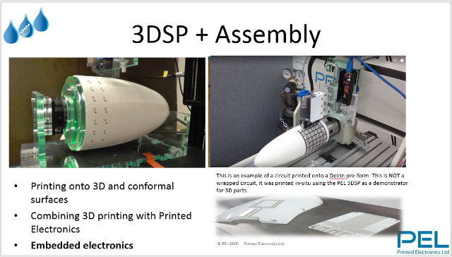
Figure 5 Examples of parts printed using PEL's 3DSP multi-axis print system The PEL 3DSP platform is a non-contact viscous paste printer with a large 600 x 500 x 250mm print area and a four-axis motion controller. We have used it for printing antennas, FSS (frequency selective surfaces) and similar patterns onto various external surfaces on parts. The system has been designed for both conductive printing and material deposition. In the area of material-deposition we partner with a UK 2D-material manufacturer to improve structural strength of industrial composites by directly printing. |
|
|
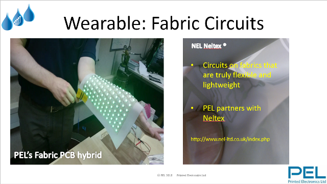
For conformal systems with five and more axes of control PEL partner with Neotech AMT GmbH whom have a system which allows printing of, for example, mobile antennas directly on casing elements. Our 3DSP system is a conformal printer, meaning it prints on the surface of existing parts. But printing only on the surface means that the circuitry then needs to be further protected by additional coatings. To truly embed the electronic interconnects inside a 3D printed object during its manufacture, PEL are partners in an Innovate UK funded project called IMPACT which will further develop our print head system in collaboration with UK 3D Printer manufacturer CEL, Iterate Design and Warwick University’s WMG. The IMPACT project will deliver a unique large format FDM print platform that incorporates conductive deposition concurrently with the 3D printed parts. I have argued that form-factor is the main differentiator for printable and additively manufactured electronics – and nowhere is that more true than in wearable electronics. By wearable here, I do not mean items of small rigid electronics in the form of a watch, or a health tracker, I refer to circuits that need to be flexible in the same way that clothing fabric is flexible: bendable, perhaps stretchable and certainly able to be scrunched in ways that conventional electronics cannot be (and still survive). PEL have partnered with NEL (www.nel-ltd.co.uk), patent holder of the fabric circuit technology, for a number of years and have used this PCB-like material in a wide range of designs from flexible heaters to small displays, fashion-based electronics and LED matrix displays that have even been flown and tested on drones. |
|
|
Figure 6 An example of a PEL fabric circuit - an addressable LED display array on a soft flexible fabric. Wearable electronics on fabrics has potential to be used in areas of assisted living and healthcare, so is an area of focus. PEL are partners in three-year EU Horizon2020 project called Maturolife, led by Coventry University (https://cordis.europa.eu/project/rcn/212827_en.html). The aim of this project is to create electronics for assisted living in an unobtrusive form factor where the sensors are integrated into everyday garments in a form factor unnoticed by the wearer. An extension to fabric materials is Soft Materials, a highly innovative branch of printable electronics that incorporates electronic materials that are truly flexible, stretchable and compatible with being used both on and inside the human body. A number of academic groups work in this area but the pioneering work of the Takao Someya Research Group at the University of Tokyo (http://www.ntech.t.u-tokyo.ac.jp/en/ ) and Professor John A. Rogers at Northwestern University in the USA http://rogersgroup.northwestern.edu/ stand out. These groups and commercial spin-outs have demonstrated a diverse range of processes and products including conformable membrane electronics directly applied to skin and even heart tissue, through to high volume commercial UV sensors with L’Oréal that are the size of a fingernail and can be read with a smartphone. In conclusion, I hope I have shown that the field of Printable Electronics is wide, has unique capabilities and is not directly competitive to the existing interconnect industry. Nor is it simply a way of making lower cost versions of existing product. Instead, it is a means to realise electronic circuitry in new and very different form factors. |
| Section 10 |
Industry News |
| Section 10.1 |
PCB Manufacturer BATM Systems SRL, Romania re-certified to ISO 9001:2015
Waterlooville, UK, 16 May 2018 -- SCL PCB Solutions Group, a leading European manufacturer of PCB requirements, announced that its Central European facility located in Craiova, Romania has been successfully re-certified with zero non-conformities to ISO 9001:2015, the international standard for a quality management system. About BATM Systems SRL BATM Systems SRL is a mid to high-volume PCB manufacturing facility in Craiova, Romania and as a wholly owned subsidiary of Spirit Circuits is part of the SCL PCB Solutions Group. Officially opening its doors May 2017, it is the first volume PCB manufacturing plant to be established in Romania and offers short lead-times, competitive pricing and a fully controlled and reliable supply chain. |
| Section 10.2 |
Ventec Launches Dk 3.48 Ceramic-Filled Hydrocarbon Thermoset Materialtec-speed 20.0: Designed for the world's most demanding high frequency PCB applications
About Ventec International |

|
Corporate Members of The Institute of Circuit Technology May 2018 |
||
| Adeon Technologies BV |
Weidehek 26,A1 4824 AS Breda,The Netherlands |
www.adeon.nl |
| ALR Services Ltd. | Unit 9, Thame Business Park, A1 Thame, Oxon OX9 3XA | |
| Atotech UK Ltd. | William Street, West Bromwich. B70 0BE | www.atotech.com |
| CCE Europe | Wharton Ind. Est., Nat Lane, Winsford, CW7 3BS | www.ccee.co.uk |
| ECS Circuits Ltd. | Unit B7, Centrepoint Business Park, Oak Road, Dublin 12, Ireland | www.ecscircuits.com |
| Electra Polymers Ltd. | Roughway Mill, Dunks Green, Tonbridge, TN11 9SG | www.electrapolymers.com |
| The Eurotech Group | Salterton Industrial Estate, Salterton Road, Exmouth EX8 4RZ | www.eurotech-group.co.uk |
| Exception PCB Solutions | Ashchurch Business Centre, Alexandra Way, Tewkesbury, Gloucestershire. GL20 8NB | www.exceptionpcbsolutioncom |
| Merlin PCB Group | Hawarden Industrial Park, Manor Ln, Deeside, Flintshire, North Wales, CH5 3QZ | www.merlinpcbgroup.com |
| Faraday Printed Circuits Ltd | 15-19 Faraday Close, Pattinson North Ind. Est., Washington. NE38 8QJ | www.faraday-circuits.co.uk |
| Graphic plc | Down End, Lords Meadow Ind. Est.,Crediton EX17 1HN | www.graphic.plc.uk |
| GSPK (TCL Group) | Knaresborough Technology Park, Manse Lane, Knaresborough HG5 8LF | www.gspkcircuits.ltd.uk |
| Invotec Group Ltd | Hedging Lane, Dosthill, Tamworth B77 5HH | www.invotecgroup.com |
| PMD (UK) Ltd. | Broad Lane,Broad Lane,Coventry CV5 7AY | www.pmdgroup.co.uk |
| Rainbow Technology Systems | 40 Kelvin Avenue, Hillington Park, Glasgow G52 4LT | www.rainbow-technology.com |
| SCL PCB Solutions Group | 22-24 Aston Road, Waterlooville, Hampshire PO7 7XJ | www.spiritcircuits.com |
| Stevenage Circuits Ltd | Caxton Way, Stevenage. SG1 2DF | www.stevenagecircuits.co.uk |
| Ventec Europe | 1 Trojan Business Centre, Tachbrook Park Estate, Leamington Spa CV34 6RH | www.ventec-europe.com |
| Zot Engineering Ltd | Inveresk Industrial Park Musselburgh, B19EH21 7UQ | www.zot.co.uk |