
Journal CSS

The Journal of The Institute of Circuit Technology Vol 13 No 1 March 2020 |
|
| Links to Contents |
Section |
| 1 | |
| 2 | |
| 3 | |
| 4 | |
| 5 | |
|
Prof Barrie Dunn at "IMPACT Europe" on 3-4 December 2019 in Brussels |
6 |
| 7 | |
|
Development and processing of an ink jettable soldermask and advantages of use in PCB manufacture |
8 |
| 9 | |
| 10 | |
| 11 | |
| 12 | |
| Section 1 |
Calendar of Events |
| Date | 2020 Events |
| 25th February | AGM and Evening Symposium |
| 6th - 9th April | Annual Foundation Course - Chester - POSTPONED |
| 2nd June | Annual Symposium at the British Motorcycle Museum - POSTPONED |
| 8th September | Autumn Seminar -Tewkesbury |
| TBA November | Winter Seminar - Hartlepool |
| Section 2 | Editoral |
|
Editorial |
12th March 2020 Having recently being honoured with becoming the Chair of the ICT, I have been asked to write the editorial for this issue of our journal. I had been pondering this since taking on the position a couple of weeks ago and had been planning on writing about the things I would like to achieve as the Chair this year, but as the days have progressed I realised that I have to now open with the uncertainty we all face related to COVID-19. It feels that even if we are lucky enough to find our personal health unaffected, our businesses will certainly be impacted by it. Yesterday, I had a day trip to Dusseldorf, for a client meeting, and the airports were like ghost towns. Today, I am in London for a board meeting for Electrical Safety First, a charity that I am a trustee of, and even London is much quieter than normal….no fight to get a seat on the train to Waterloo, which is unheard of! Many people seem to have hit the pause button on life (well except for buying toilet rolls, it seems). Whatever our personal opinion is of the situation, whether it be an over-reaction, the government not doing enough, or something in-between, it leaves us with a challenging year ahead, but maybe some longer-term opportunities too. Will our customers / suppliers start to think twice about having an over reliance on sourcing products from just one country, or even just one region of the world? Will those who already had this security of supply prosper from it and be held up as examples to what all should aspire to? Questions that I suspect we will only find the answers to in the coming months and years, but I hope the answer will include a reinvigoration of British manufacturing. The one good thing we can say in the UK though, is that within our PCB industry we have a lot of friends and even though many may be competitors, we know that when the chips are down, we will always help each other out. The ICT members and the reinvigorated Fabricators' Group are perfect examples of this. When we need support, we know that we have friends to turn to and at this time, this is something that we cannot put a price on. I will briefly mention what I had started to consider writing in this editorial, as I think it is still relevant and something I hope that we can work towards after the dust has settled, and that is sharing the amazing depth of experience we have in this industry with the next generation of PCB engineers. The ICT hold its Foundation Course on an annual basis (our 40th anniversary event has just, today, been postponed until August, for all of the reasons mentioned above) with this same noble aim but we, as an industry, need to do even more. I sat in our last evening seminar at Meriden, listening to some fascinating presentations, and when I cast my eye around the room I realised the true wealth of knowledge that was present, but also how we are an aging community (no insult intended to those that were there, I consider myself in that same aging bracket these days!) and that if we do not find additional ways to pass on our knowledge to the next generation, the UK PCB industry will be so much poorer and weaker for it. I hope with everything going on that you can find time to enjoy this journal. My thanks to all the contributors and to the ICT team that help to put this together, voluntarily, in their own time. Hopefully, you will pass it on to some of the younger members of your team and consider bringing them along to the next ICT event. And finally, may I wish you and yours good health during these challenging times.
|
| Section 3 |
ICT Council Members |
| Council Members 2020: |
Emma Hudson (Chair), Andy Cobley (Past Chairman), Steve Payne (Deputy Chairman), Chris Wall (Treasurer), William Wilkie (Technical Director, Membership & Events), Richard Wood-Roe (Web Site), Lynn Houghton (Hon Editor), Matthew Beadell, Martin Goosey, Maurice Hubert, Lawson Lightfoot, Peter Starkey, Francesca Stern and Bob Willis, |
| Section 4 | Membership News | |||
| 4.1 | New Members |
|||
| Bill Wilkie: Technical Director and Membership Secretary | Re-Instatement | |||
| 10311 | Leigh Allinson | Ventec | ||
| 10310 | Alan Green | Eurotech | ||
| 10030 | Graham Temple | Eurotech | ||
| Go back to Contents | ||||
| Section 5 |
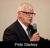
The Institute of Circuit Technology Evening SeminarHarrogate, 5th December 2019 Pete Starkey |
|
|
Since 2016, the Institute of Circuit Technology (ICT) has held its Northern area Christmas seminar at the Majestic Hotel in Harrogate—the elegant and historic English spa town in North Yorkshire. I commented last year that the Victorian splendour of the palatial and stately Majestic was steadily deteriorating. The current owners apparently shared that opinion and have driven it back up-market with a £15M makeover and a new spa. It was a very nice conference venue, but overnight accommodation was now rather pricey for many of the participants who chose to stay elsewhere. |
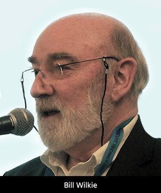 |
Delegates travelled from far and wide, some from overseas, to attend this popular ICT event, expertly organised by technical director Bill Wilkie. He welcomed all participants, acknowledged the generous support of FineLine Global, and reported the success of the new-look Journal, which included a voice-over PowerPoint of Frank Ferdinandi’s presentation at the Meriden seminar. He believed that features of this type would particularly benefit members as far away as St. Petersburg and California, who did not have the opportunity to attend in person. |
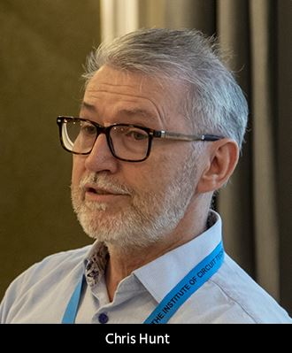 |
A reminiscence from the days of spin-coating photoresists, and accidentally coating his trousers, provided Wilkie with a tenuous connection for introducing his first speaker, Dr. Chris Hunt from Pireta, to discuss how harnessing circuit board technology could revolutionise the e-textile technology and wearables market. With a background of over 40 years as a leading research scientist at the National Physical Laboratory, Dr. Hunt had set up Pireta to develop the concept of integrating functional electronics into wearable textiles without affecting their handle, drape, stretchability, or breathability. The approach was radically different to processes that used printed conductive inks or stitched conductive thread into fabrics and was based on the principle of bonding a thin metallic layer on to the fibres of the textile, using commercially available chemistry; this resulted in the textile itself becoming conductive at fibre-level with no impact on its desirable physical properties. Pireta had patented a fully additive nanoparticle catalytic bonding process for applying copper to individual textile fibres, with a process sequence resembling that used in the metallisation of PCBs. The fabric was initially conditioned with a sodium hydroxide-based solution, and then activated with a cationic polyelectrolyte linking agent. Nano-metal particles were attached using a printing process, followed by building-up a metallic layer by electroless plating and final passivation by metallic or organic coating. Dr. Hunt’s examples involved silver nanoparticles, which were produced by the reduction of silver nitrate in solution, existing initially as 20-nanometre particles, aggregating at the surface to 50–100 nanometres, and acting as sites for the deposited metal to grow. The process was applicable to a wide range of fabrics—knitted, woven or non-woven, natural or synthetic—and resulted in a highly conductive deposit, even at radio frequencies, with robust wash, stretch, and fold performance. Large areas could be rendered conductive if required, complex designs could be patterned by a simple printing process, and the fabric could be dyed afterwards. Dr. Hunt also showed a video demonstrating “truly wearable technology,” with the versatility to be employed “on any textile, at any stage, on any scale, and in any sector.” Applications are proliferating, and the global smart textile market is projected to exceed $5B by 2022' |
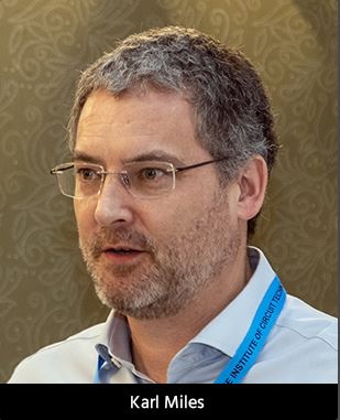 |
Print your own circuit boards! The second presentation came from Karl Miles, technical sales manager with Peak Group—U.K. distributors for the Voltera V-One desk-top package for prototyping single- or double-sided PCBs. Designed to be quick and simple to operate with a straightforward user interface, the integrated package was a dispenser-based printer capable of operating with cartridges of conductive ink or solder paste with a maximum print area of 5.0” x 4.1” and minimum track and gap 0.008”, working from a conventional Gerber input. The standard substrate was unclad FR-1 paper-phenolic laminate, available in a range of sizes from 3” x 2” to 5” x 4” and thicknesses up to 3 mm, including templates for Arduino and Raspberry Pi projects. Unclad FR-4 laminate could be used in applications where drilling was not required. The system had a heated platen capable of reaching a maximum temperature of 240°C in about two minutes. Curing the silver-based conductive ink was accomplished in 30 minutes at 200°C. Once the first side had been cured, it was possible to print a second-side pattern to yield a two-layer circuit. Interconnection between the two sides could be achieved using metal rivets in drilled holes, and a bolt-on CNC drill attachment for FR1 was available for drill sizes from 0.7–1.6 mm. In its alternative mode, the printer could be used as a solder-paste dispenser for pad sizes down to 0402, using a cartridge of tin-bismuth-silver paste. After hand-placing the components, the assembly could be reflowed using the same heated platen as used for curing the conductive ink. As a means of taking breadboard projects to the next level, the system had appealed to academic and educational establishments, hardware startups, and other companies that needed rapid, low-cost prototype circuits and assemblies. |
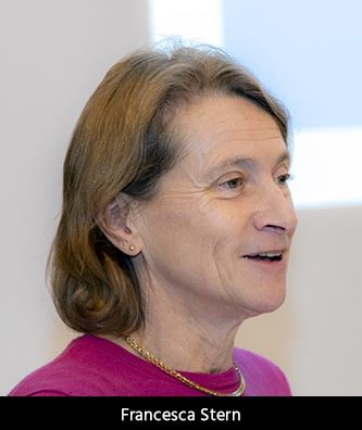 |
Next, two eagerly awaited analyses of trends in the global electronics and PCB industries were presented. The first was from Francesca Stern, ICT council member, the second from Walt Custer, ICT member, who apologised that because of ill-health, he could not be present but had delegated his presentation to Alun Morgan, chairman of EIPC. Francesca Stern started with her end-of-year round-up. According to Office for National Statistics figures, 2018 had been a good year for U.K. electronics production with an average growth of 14%, although it was likely that the 2019 figure could be as low as 2%. Germany had shown negative growth for the first half of 2019, but the situation was improving slightly. In Eastern Europe, Hungary and Poland had remained positive. Growth in electronics production in the USA had declined from 6.2% in 2018 to 2–3% in 2019, and the Japanese industry had gone negative. No current figures were available for China, but it was known that base-station production had plummeted. Looking at printed circuit production, the value of the PCB market in the U.K. in 2018 was £199M, of which £129M was manufactured domestically. The corresponding figures for 2019 had been estimated as £179M and £110M. The estimate for world PCB production in 2018 was £49.7B ($66.3), of which China 54%, Taiwan 12%, South Korea 11%, North America 5%, and Europe 3.5%. Europe was showing negative growth—particularly Germany—the USA was trending in that direction, and there were pessimistic forecasts for Japan. |
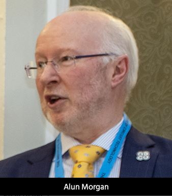 |
Walt Custer’s analysis, presented by Alun Morgan, showed a similar pattern. Global growth had been slowing, the main issues being tariffs, trade disputes, and uncertainty in Europe regarding Brexit. As a consequence of trade disputes, production in Asia was being moved around. For example, Taiwanese companies were moving manufacturing out of China. And disruption could continue for years to come. Global purchasing managers’ indices were “useful but sobering leading indicators” and indicated no growth, whereas those for Europe showed a definite contraction, especially Germany. Although volume markets were currently flat, emerging markets included autonomous cars, internet of things (IoT), industrial internet of things (IIoT), cloud storage, 5G handsets and infrastructure, virtual and augmented reality (VR and AR), artificial intelligence (AI) and machine learning, smart cities, smart agriculture, drones, robots, wearables, 3D printing, and health care. Looking at the value of world PCB production in 2018, Haiyo Nakahara’s estimate was $74.5B, with China’s share being 54.4%, America 4.2%, and Europe 3.1%. Michael Gasch’s figure for Europe was €1921M, Germany accounting for 43.7% of this total, and the U.K. at 8.7%. Gasch had commented that Europe will most likely close 2019 10% down against 2018. The number of PCB shops in Europe has declined since 2012 from 284 to 202 in 2018, mainly the smaller sub-€10M shops, although the number of staff employed had remained fairly steady in the 16,000s. |
|
Hans Friedrichkeit believed that an economic turnaround had probably been reached, with the first glimmer of hope in the German industry. The downturn in incoming orders had slowed, although production was likely to fall further in the short term due to the decline in past orders. He considered that the automotive industry was likely to stabilise, since new car registrations in Germany had risen by 3% year-to-date, and PCB companies with a high share in the automotive industry would benefit. Globally positioned and technologically highly differentiated PCB manufacturers saw their earnings more than halved versus the previous year, but for 2019 as a whole, sales were expected to remain at 2018 levels, with a positive outlook. “It looks as if the bottom of the economic valley of tears has been passed.” |
|
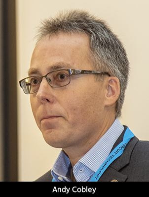 |
Professor Andy Cobley, ICT chairman, brought proceedings to a close, thanking speakers for sharing their knowledge and experience, delegates for their attention and support, FineLine for their kind sponsorship, and giving a special thanks to Bill Wilkie for his smooth and professional organisation of another successful event. The networking continued over a convivial Christmas-themed supper. |
|
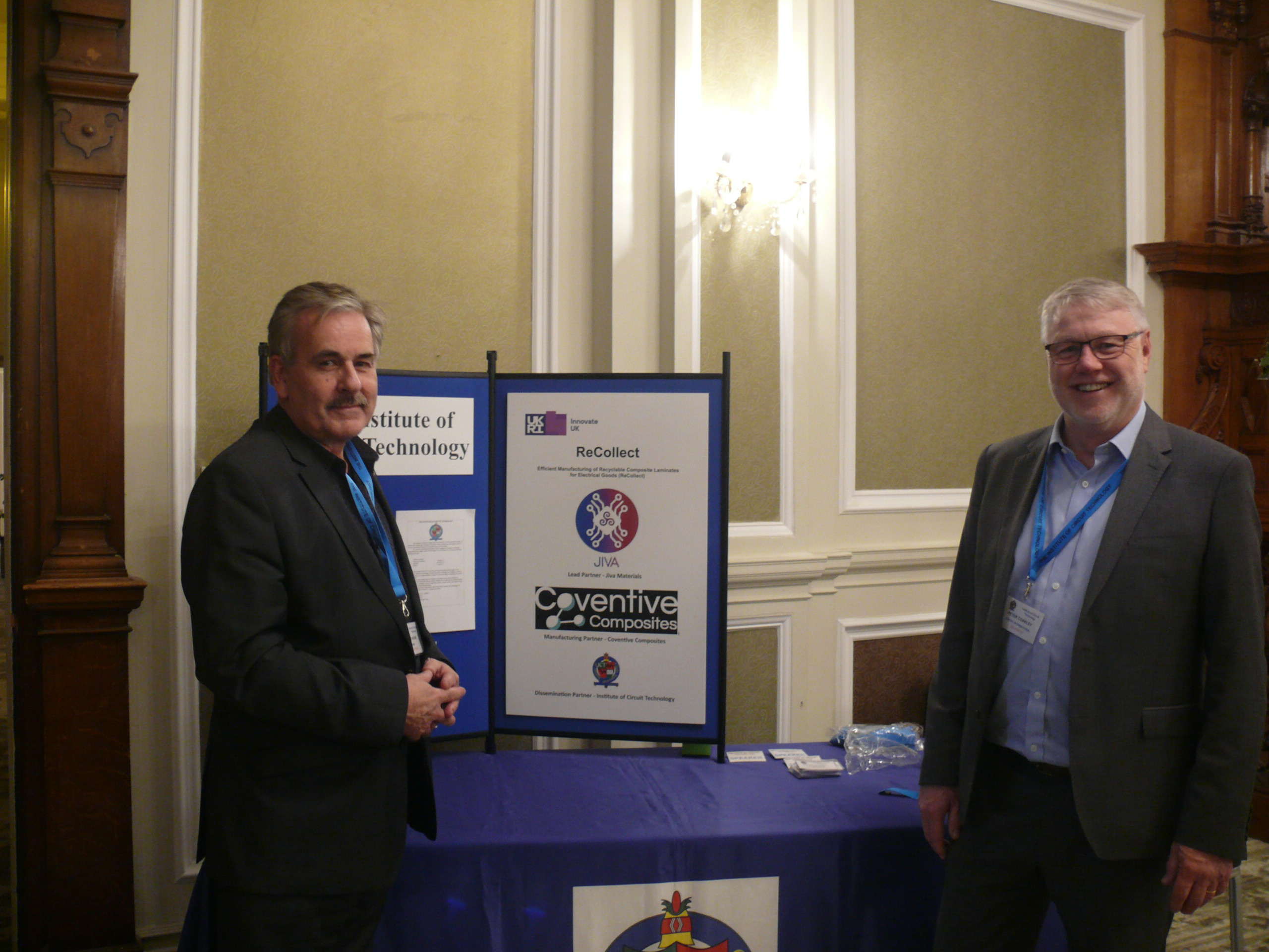
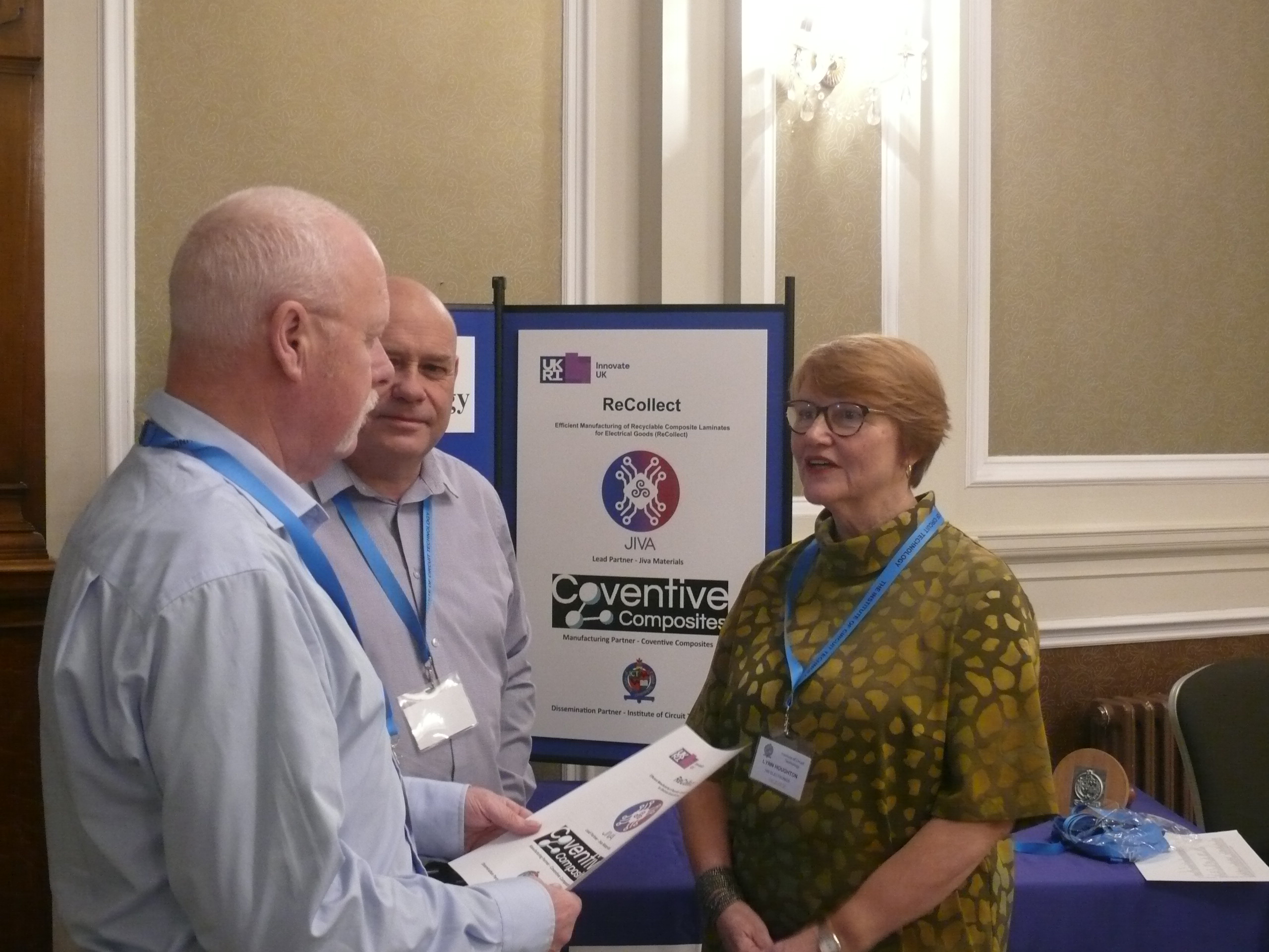
ReCollect Efficient Manufacturing of Recyclable Composite Laminates for Electrical Goods Recollect is an Innovate UK funded project, to develop and exploit fully recyclable substrates for the Electronics Industry. The ICT are Dissemination Partners with Jiva Materials the Lead Partner and Coventive the Manufacturing Partner
Steve Payne, ICT council discussing the Recollect Project with Peter Coakley of Ventec International, suppliers of base laminate.
|
|
|
Lawson Lightfoot, ICT Council, Lynn Houghton, ICT Journal Editor, discussing the Recollect project with Erik Butchert, CCI Eurolam, suppliers of base laminate. |
|
|
Reproduced by kind permission of I-Connect007. I am also grateful to Alun Morgan for allowing me to use his photographs. Pete Starkey December 2019 |
|
| Section 6 |
"IMPACT Europe" 3-4 December 2019 - Brussels Prof Barrie Dunn |
|
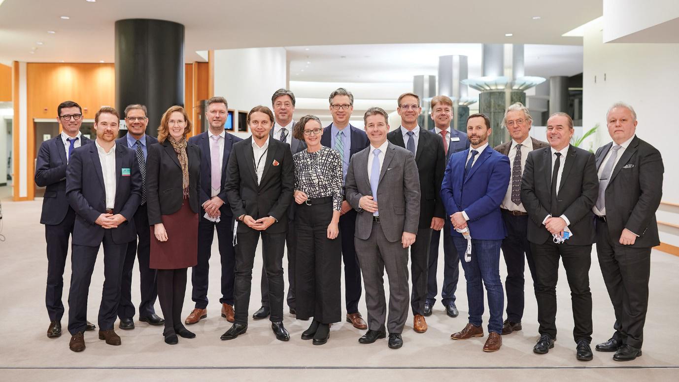
Professor Barrie Dunn, School of Engineering at UoP, is a member of the Lead-free Risk Management (PERM) Council with the 'Association Connecting Electronics Industries (IPC, formerly called the Institute of Printed Circuits)'. He was invited to join IPC’s Government Relations team for the annual flagship event called IMPACT Europe on 3-4 December 2019 in Brussels. Barrie's involvement with IPC spans more than 30 years, covering his employment in the Netherlands, as Head of the Materials and Processes Division with the European Space Agency (ESA), and now as Honorary Professor with UoP. The agenda included several important and relevant topics relating to the European electronics industry: In the South of England, notably in the Portsmouth area, electronics manufacturers constitute a major boost to the UK economy. Local industries cover the whole spectrum, from aerospace and defence, advanced manufacturing, agriculture to consumer electronics. This IMPACT event is significant for British and EU electronic manufacturers and research groups as it is an opportunity for them to provide information to the legislators of EU industrial policy. Objectives appear to be shifting from pure waste management to the sustainability of electronic materials from waste by various metallurgical extraction processes; here the impact will be on secondary raw materials which are strategically important for the future. Ideas for the recovery of common metals and rare earth metals from e-waste will be needed from research groups. The topic of ‘urban mining’ was covered - materials of value might be extracted from existing scrap yards and land-fill sites.
Group photo (IPC members with, at centre, 4 MEPs); Barrie Dunn is located as third from the right-hand-side.
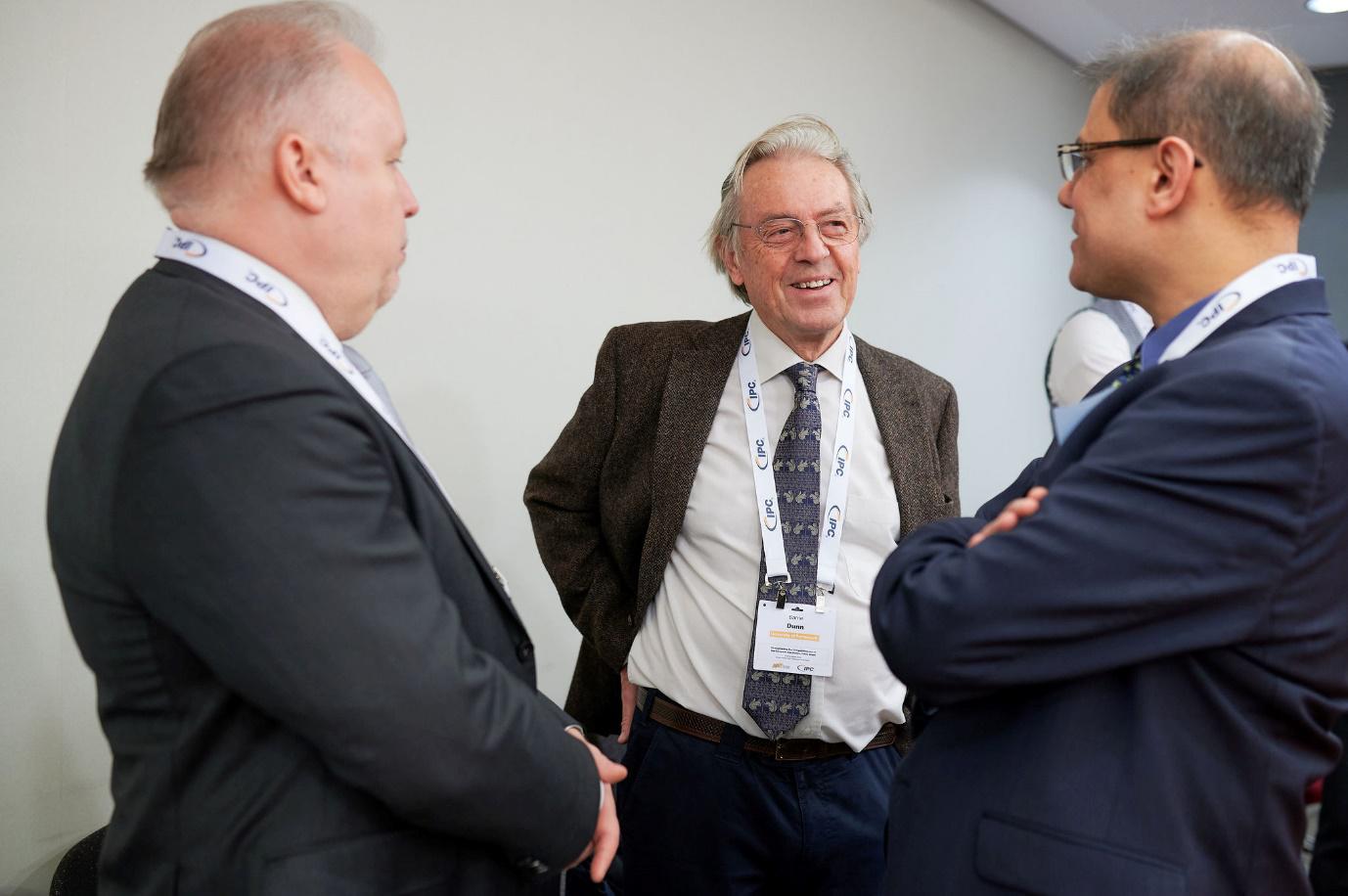
Barrie Dunn with colleague delegates from Estonia (left) and the IPC. |
|
| Go back to Contents |
| Section 7 |
Institute of Circuit Technology Spring Seminar 25th Feb 2020 Pete Starkey |
 |
Back to Meriden, the nominal centre of England. The daffodils were blooming, although the weather was hardly spring-like: cold, blustery, and rivers bursting their banks. Some had to take substantial detours to avoid flooded roads, but members of the Institute of Circuit Technology (ICT) are robust and resilient! A good crowd made it to the seminar that followed the annual general meeting of the ICT, with five specialist presentations and excellent opportunities to network with their peers in the industry. |
 |
In his welcoming remarks, ICT Technical Director Bill Wilkie commented that the Institute continued to attract new members—membership currently totals over 400—and that the Annual Foundation Course remained an especially popular educational event, introducing the technology to generation after generation of printed circuit engineers and technicians. The Foundation Course had originated 40 years ago, organised by the Northern U.K. Printed Circuit Group, and held at the Hewlett-Packard facility in South Queensferry. He acknowledged the companies who continued to support the course and presented commemorative plaques to David Douglas, managing director of the Eurotech Group, and Neil Martin, chairman of the Merlin PCB Group. |
|
Chris Wall Technical Director Electra Polymers and Chemicals |
Wilkie had once more coordinated an excellent seminar agenda. He introduced as his first speaker Chris Wall, technical director at Electra Polymers, who gave a detailed review of the development and processing of an inkjettable solder mask and discussed the advantages of using it in PCB manufacturing. An understanding of the inkjet application process was the fundamental first step in the development programme, and Wall gave a brief introduction to the types of print-head available and how ink-drops were generated. This gave a good insight into the factors constraining the formulator, particularly the limited choice of suitable raw materials compared with those associated with conventional solder masks, restricted to very low viscosity resins and monomers and pigments with nanoscale particle sizes. Furthermore, it was necessary to keep filler content low or absent, which led to further challenges in achieving acceptable flammability, thermal shock, and solder resistance. Formulations also included flow agents, surface property modifiers, photoinitiators, and thermal curing agents. Optimum viscosity varied according to the type of print head, and—in combination with surface tension—affected jetting performance according to some complicated fluid dynamics where stable drop formation was a function of Reynolds number, Weber number, and Ohnesorge number. Wall did not dig too deeply into the physics. And once the ink hit the surface, its wetting characteristics and factors like contact angle affected spreading, bleed, and track-edge thinning, as well as the coating performance of any subsequent layers deposited. The curing mechanism depended on the resin chemistry, and inkjet formulations were generally pin-cured with UV during the printing operation to effectively set the image. A final thermal cure completed the crosslinking reaction. Once a test product had been formulated, it would initially be screen printed to assess its basic solder mask properties, and modified as necessary before being evaluated for its jetting performance and the properties of the jetted coating after curing. The sequence would be repeated as many times as necessary while the formulation was fine-tuned and optimised. Attributes—such as solder dam resolution, resistance to multiple solder reflow cycles, compatibility with plating chemistry, and conformal coatings—would be ascertained before submitting the final formulation for external testing for compliance with UL 94V0, RoHS, IPC-SM840, NASA specifications, etc., as well as automotive standards and individual customer requirements. Wall summarised the advantages of the inkjet process over the liquid photoimageable route, particularly in the elimination of the coating, drying stages, exposure and development stages, the savings in space, water and energy costs, and the lack of solvent emissions. There was no undercut at image edges, and—therefore—no risk of chemical or flux entrapment. He emphasised that inkjet solder mask relied on good surface preparation for adhesion, chemical resistance, and print quality. |
 |
A consequence of the continuing evolution of technology in the electronics industry was the production of e-waste from end-of-life equipment. It had been estimated that the U.K. produced over 500,000 tonnes annually of waste from electrical and electronic equipment (WEEE), of which over 40,000 tonnes originated from IT and telecoms equipment. Toxic components in WEEE could cause environmental problems if not properly managed; conversely, WEEE contained valuable metals that could potentially be recovered and recycled as raw materials. Indeed, in the case of printed circuit assemblies, the metal content of the waste was higher than in natural metal ores. For example, one tonne of WEEE could contain gold worth around £45,000. A current project at Coventry University focused on the recovery and recycling of metals from waste printed circuit assemblies as a step towards the circular economy and the sustainability of critical raw materials. Daniel Ray introduced the concept of “urban biomining” as an alternative to the traditional methods of recycling: pyrometallurgy—which involved high temperatures for pyrolysis or smelting—or hydrometallurgy—which utilised chemicals such as acids and cyanide. Neither was considered environmentally sustainable in today’s climate, and bioleaching had been identified as a way forward. |
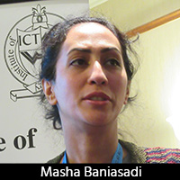 |
Biomining? Bioleaching? Science fiction? Dr. Mahsa Baniasadi explained that biomining offered a cost-effective and environmentally friendly option for leaching metals from ore using microorganisms to convert solid metals into aqueous species, and was already used to produce about 5% of the world’s gold and 20% of the world’s copper. The objective of urban biomining was to use spent electronics as the feedstock to make fresh electronic components, employing synthetically enhanced microbes to biologically extract specific metals. As an illustration of current recycling rates, a standard periodic table had been highlighted in different colours to indicate end-of-life recycling input. Copper, silver, and lead were all above 50%, but there was a very low input of many endangered elements. The natural sources of these elements were limited and not located in the U.K., so there was plenty of scope for recycling and sustaining the supply of critical raw materials. Dr. Baniasadi briefly explained the terminology and some of the mechanisms relevant to bioleaching; for example, redoxolysis referred to oxidation-reduction reactions catalysed by bacteria, acidolysis was the production of biogenic acid, and complexolysis was the production of biogenic complexing agents. She discussed iron oxidation, sulphur oxidation, and biogenic cyanide. Once a metal was in solution, electro-winning techniques could be used to deposit it in a relatively pure state. Daniel Ray described a process for gold bioleaching using thiourea—a less harmful alternative to biogenic cyanide, and indium bioleaching from display screens using an acidolysis bioleaching mechanism. Future work planned included reuse of materials, precious metal recovery, genetic modification of bacteria, and large-scale application of the technology. |
 |
Newly appointed Chair of the ICT, Emma Hudson provided delegates with a comprehensive first-hand update on current IEC and UL standardisation work. The scope of IEC TC 91—the technical committee for electronics assembly technology—was to establish international acceptance for standards and guidelines in electronics assembly technology. ICT_Emma_Hudson200.jpgHudson is convenor of the IEC TC 91 working group responsible for preparing international standards on design, manufacturing, and testing of electronic assemblies—including the requirements and tests for materials and components used to manufacture circuit boards and electronic assemblies, as well as the formats of electronic data and libraries for describing these products and processes. She showed a long list of recent publications, with items of interest highlighted. There were 29 documents currently being worked on—24 new and five being revised, of which 20 were standards, and three were technical reports. Hudson is EIPC’s representative on the UL Standards Technical Panel for the UL 796, UL 796F, UL746E, and UL 746F standards. Probably the most relevant upcoming proposal from UL was to rename “solder limits” as “assembly soldering process” to provide a clearer interpretation of the significance of the parameter in representing the soldering processes the PCB would be exposed to during component assembly operations. New limits followed research from FED and ZVEI, and the proposed default condition would be six cycles of IPC-TM-2.6.27 T260 reflow, or a special reflow profile if agreed with the OEM or ODM. The reflow profile would be considered representative of wave and selective soldering, and UL’s follow-up service inspectors would check the maximum reflow temperature and the number of soldering cycles that the assembly was exposed to, but would not be checking details of the reflow profile beyond this. There was no plan to retrospectively apply the new assembly soldering process limits to existing board types—only to new evaluations, once the proposal had been accepted and added to UL 796, UL 746E, UL 796F, and UL 746F. And there was no guarantee that the proposal would be accepted by the UL Standards Technical Panel, although it was expected to happen with the coming 6–18 months. A significant new proposal presented at the UL Standards Technical Panel meeting came from Alun Morgan, representing Ventec. He suggested that the STP consider defining laminate groups by performance instead of nominal chemistry, to align with the industry and help designers in specifying their PCB requirements. |
 |
Dr. Jonathan Swanston, chief technical officer with Jiva Materials, gave an update on the ReCollect project, funded by Innovate U.K., and focused on the efficient manufacturing of recyclable composite laminates for electrical goods. Jiva Materials was one of three project partners—the others being Coventive Composites, an independent provider of expert services relating to composite materials, and the ICT, supporting dissemination and industry feedback. Jiva had developed the world's first fully recyclable PCB laminate. He passed around samples of his material, composed of a natural fibre bound with a polymer soluble in hot water but not in cold water, which had the appearance of a light-brown-coloured unclad laminate. Dr. Swanston reviewed some statistics which indicated that PCBs made up 8% of the 50 million tonnes of electronic waste that was generated in 2018. The ReCollect project explored an alternative way of managing end-of-life circuit boards. Currently, the only practical way of recycling glass-epoxy circuit boards involved shredding and incineration to recover the metal content. The ultimate aim of the project was to remove glass-epoxy boards from the supply chain, by demonstrating that Jiva’s Soluboard® could match the performance of CEM-1 and FR-4 materials. Dr. Swanston explained that Soluboard was a fully biodegradable and non-toxic product based on flax. A primary aim of the project was to demonstrate the feasibility of producing the material in high volumes at a competitive price, using a continuous-production process in development by Coventive Composites. The nature of Soluboard® was to delaminate when immersed into hot water, enabling the flax fibres to be composted or repurposed and the electronic components to be removed for reprocessing. Silver printing was a feasible method for creating functional circuits. But to use existing aqueous manufacturing processes, it was necessary to seek a means of chemically protecting the material in-process, and this was part of the project. Dr. Swanston commented that “white goods”—large household appliances—constituted more than 30% of e-waste, and that the Global E-Waste Monitor had reported that less than 20% of this was documented as collected and recycled. The rest went to landfill. Jiva intended to push for the safe recovery of e-waste in line with the WEEE2 Directive. The white goods market was their initial target, and specifications from potential customers had defined electrical, flammability, and mechanical requirements. Soluboard® had a Tg of 126°C and a UL94V0 flammability rating. Its electrical properties were being determined by a third-party laboratory, and final results were awaited. As part of the project, functioning populated PCBs would be designed, manufactured, and evaluated as specified by end customers. |
 |
Government policy clearly aims to end the sale of new diesel and petrol cars by the year 2035 and compel the mass adoption of electric vehicles. The cost of the battery currently represents a significant proportion of the overall cost of an electric vehicle; the battery gradually loses its capacity and is typically replaced when it drops to below 70–80% of the original. The first generation of vehicle batteries are reaching end-of-life now, and volumes are set to increase significantly. To reuse in secondary applications or to recycle to recover raw materials were questions explored in an informative presentation from Professor Martin Goosey. In the context of a circular economy, it made sense to reuse and then recycle, but both possibilities had some merits. The number of end-of-life vehicle batteries was predicted to grow from 55,000 in 2018 to 3.4 million by 2025 and 6.0 million by 2030, and this represented around 275 gigawatt-hours of capacity. Should electric vehicle batteries be used for home energy storage, and was this an economic proposition for the average user? Tesla, for example, manufactured rechargeable lithium-ion batteries for stationary energy storage but preferred to recycle its used batteries. Although there were several nominal benefits of reusing vehicle batteries, the negatives included transport costs and the costs of dismantling, testing, reassembly, and certification. There were many different types of battery chemistry and size, and although reuse would nominally extend the life, the batteries would ultimately need recycling anyway. The need to balance power availability was becoming more important with the growth of electricity generation from intermittent sources; for instance, the solar industry heavily depended on the cost-effective integration of appropriate energy storage systems. Battery performance was continuously improving, and new battery costs were reducing. The example quoted by Professor Goosey indicated that the cost per kilowatt-hour in 2020 was 20% of the 2010 figure, projected to fall to 10% by 2030. Why not just use new batteries and simply recycle the old ones? The best route was still to be determined. However, with the move to electric vehicles being accelerated by government policy, it would be vitally important that the correct decisions were taken. Click here to view PDF presentation Professor Goosey wrapped-up the proceedings, thanking all of the participants. He also gave a special thanks to Bill Wilkie for his superb organisation and management of the event. |
|
Reproduced by kind permission of I-Connect007. Pete Starkey February 2020 |
|
| Go back to Contents |
| Section 8 |
Development and processing of an ink jettable soldermask and advantages of use in PCB manufacture Chris Wall Electra Polymers Ltd |
|||||||||||||||||||||||||||||||||||||||||||||||||||||||||||||||||||||||||||||||||||||||||||||||||||||||||||
|
Chris Wall, Technical Director Electra Polymers and Chemicals |
Introduction Electra Polymers has been involved with the development and manufacture of soldermask for over 35 years. Starting with two-component epoxy based materials, through single-component UV curing products to LPISM which are still in use today. Most of these products relied on screen printing as a means of application with some formulated for application by HPLV air spray, electrostatic spray or curtain coating. First attempts to develop an inkjet soldermask were in the early ‘90s. However, the technology did not really take off then, owing to inadequate performance from the heads and printers, due in part to a lack of the computing power to drive the multiple nozzles needed. Only relatively recently has the hardware been available to make the inkjet soldermask process as a whole viable. This paper sets out briefly the methodology used to develop and formulate an inkjet soldermask, the advantages of the process over the existing LPISM process and the results achieved. |
|||||||||||||||||||||||||||||||||||||||||||||||||||||||||||||||||||||||||||||||||||||||||||||||||||||||||||
|
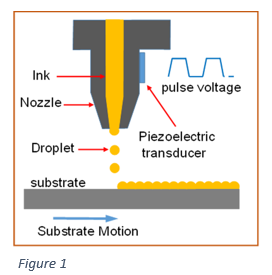
Understanding the Inkjet application process The first part of the method was to understand the ink jet application process. As mentioned above, first attempts to develop an ink jet soldermask were over nearly 30 years ago and the printhead and printer technology has moved on dramatically in that time. Printheads used today, in soldermask printing, are Drop-on-Demand (DOD), piezoelectric type. With this type of printhead a voltage pulse is applied to each nozzle, which causes the nozzle walls to flex and eject a droplet of ink. (Fig1)
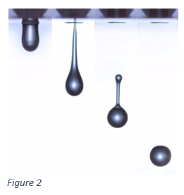
Creating the right type of pulse in terms of frequency, amplitude and duration is dependent on the acoustic characteristics of the nozzle chamber and the rheological properties of the ink and is critical to achieving good jetting performance. This is usually done by the head manufacture/printhead integrator in partnership with the ink supplier. The objective of this is to achieve the perfect ink droplet which breaks cleanly from the nozzle plate when it is ejected, with a nice clean tail, which is absorbed into the main droplet before it hits the substrate surface, thus avoiding “satellites”, small droplets which are deposited in non-image areas (Fig 2).
Heads can be non-recirculating or recirculating types and often include integral heaters to reduce the jetting viscosity of th ink. With the former, ink is fed to the head from a tank or sump, sometimes via an intermediate tank held just above the head to ensure a positive pressure to the head. Vacuum is used to prevent the ink from dripping out of the head when not printing. With a recirculating heads, as the name suggests, ink is pumped continuously throgh the head and they are somewhat more complex systems. The benefits claimed for these systems are easier priming, improved degassing and temperature control, and prevention of sedimentation of pigment. The printhead used also determines the droplet size which is jetted which in turn influences the productivity and resolution which can be achieved.
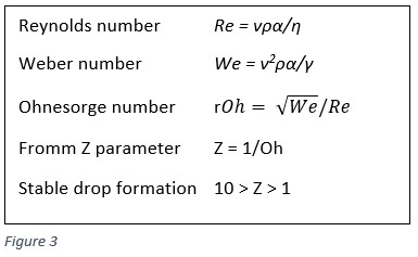
Identify Inkjet Soldermask Formulation Constraints There are a number of significant constraints on the formulator when developing soldermask for ink jet application. Viscosity requirements limit the choice of suitable raw materials. In general, only v.low viscosity resins and monomers can be used. Such materials can be more easily absorbed through the skin and care must be exercised to ensure their hazard classification is acceptable. The particle size of any pigments and fillers used is restricted to <200nm, compared to 5-15mic for conventional soldermasks. The restriction on filler size and content is a considerable hurdle for soldermask formulators as the fillers contribute to the thermal shock and solder resistance and can also reduce the flammability of the material. The ink viscosity requirements depend on the printhead being used, with recirculating heads requiring lower viscosity inks than non-recirculating heads. Surface tension of the ink is also restricted to a fairly narrow range for successful printing. and both, together with the ink density, velocity and path length are used to calculate Reynolds (Re), Weber (We), Ohnesorge (Oh) numbers and Fromm Z parameter, which are dimensionless parameters used to calculate an operating region for good droplet formation. (Fig 3).
Low viscosity materials are also more prone to pigment sedimentation and care must be taken to ensure a stable dispersion has been formed. The resulting contact angle of wet ink on substrate or cured ink can be is a useful predictor of coating performance. Choice of curing mechanism must also be taken into account; UV, thermal or some combination of both.
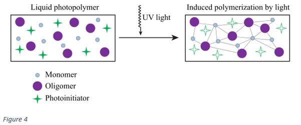
UV curing is usually preferred as it permits “pin-curing” of jetted soldermask which helps achieve good image definition (Fig 4). It can be free radical, using acrylate type monomers and resins, cationic using epoxy resins, or once again, a hybrid of both. Most soldermasks also require a thermal bake after printing and UV curing to achieve the best final cure.
Identify and source suitable candidate raw materials Once the formulation requirements and constraints have been identified and taken into account, suitable raw materials are identified and sourced. As already mentioned above, the choice of resins and monomers is restricted to those with a low or very low intrinsic viscosity to enable a low viscosity product to be produced. Any solid or higher viscosity resins can only be present in small amounts. The correct photoinitiator selection is crucial to obtaining good performance. They must combine rapid cure, to minimise the UV energy required for pin-curing (and thus avoid restrictions on print speed) as well as good through cure to avoid “wrinkling” in thicker areas, such as along track edges, and when building up thicker coats. Once again, toxicity can be a concern with several excellent initiators ruled out because of health concerns. Pigments are usually pre-dispersed in a suitable medium before incorporating them into the ink. It is essential that any dispersing agents used are compatible with the other components of the soldermask fluid and that the pigments are stable on storage in both pre-dispersion and soldermask and do not settle or separate out. The pigments themselves must be able to withstand the processing and service conditions of the soldermask and must take account of any low/no halogen content requirements. This may involve blending different pigments to achieve the required colour when no suitable single pigment is available. Other components of the soldermask may include flow agents, debubbling additives, surface property modifiers, thermal curing agents and many others dependent on the choice and skill of the formulator and the final properties desired.
Formulate Test Products The protocol used for formulating and developing an inkjet soldermask is similar to that used when formulating “standard” soldermasks:
A number of trial formulations are mixed in the laboratory. These can be quickly coated using non-jetting methods such as a wire wound rod (K-bar) to deposit a known thickness onto a test substrate. The coatings are cured different UV light sources to identify the most efficient and then baked as required for final cure. The basic soldermask properties such as solvent/chemical resistance solder resistance, hardness etc, are then evaluated. Pigment stability and hotbox stability of the test formulations can also be assessed at an early stage of the development.
Following assessment of the test formulations, poorly performing versions are eliminated or modified as appropriate and re-evaluated.
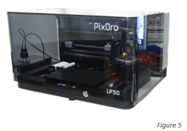
Once a number of suitable candidates are identified, these are jetted using the LP50 laboratory ink-jet printer from Meyer Berger. This printer has an integral, water cooled UV LED for pin-curing and permits a number of print settings to be modified for different formulations.
The jetting performance of the test formulations is assessed using the built-in drop watcher and by examining the resultant prints for image quality, coating smoothness and lack of “striping” and “stitching”. Effects of relatively small changes in formulation properties such as viscosity and surface tension can be easily seen. The UV energy used for pin-curing can also be adjusted and optimised for good print performance and final properties.
Using the lab printer, suitable test coupons can be printed and the cured film properties fully evaluated. As well as the basic soldermask properties assessed at the basic screening stage, coupons for Electroless Nickel/Immersion gold (ENIG), Immersion tin (Imm Sn) and Immersion silver (Imm Ag) are prepared and tested in different plating solutions.
After the jetting tests and cured coating performance results are assessed, further changes and modifications may be necessary. If so, these are made and the effects of the changes reassessed.
Once a “final” formation has been achieved, test coupons are sent to various external agencies for compliance testing to standards such as UL94 and IPC SM840.
Meeting soldermask performance requirements Throughout the formulation process, the aim is to produce a product which meets all the performance requirements of a soldermask when applied on a PCB. These are essentially the same for any soldermask, regardless of the type and application method, namely to: protect the (mainly) copper circuitry; chemically, electrically and physically from high temperatures, humidity and moisture, corrosives, dust, dirt and contamination
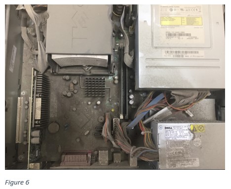
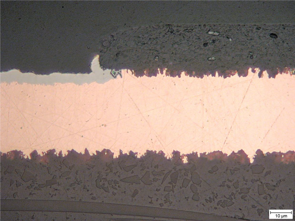
The picture in Figure 6 shows one example of why soldermask is needed! Soldermasks are also required to:
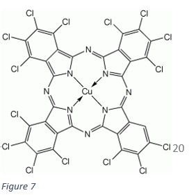
For a soldermask to be defined as halogen-free, it must contain less than 900ppm chlorine or bromine and <1500ppm total halogen. The phthalocyanine green pigments commonly used to produce soldermask contains 47-48% chlorine so, even when used at typical levels of 1% or less, contributes some 5000ppm chlorine (Fig 7). For this reason, “halogen free” soldermasks tend to be either not green, or a mixture of blue and yellow pigments to achieve a green colour.
Ideally an inkjet soldermask should also be a “universal product”, suitable for use on rigid and flexible and be suitable for use with non-recirculating and recirculating print heads
External compliance requirements Because the soldermask remains on and forms a permanent part of the PCB during its service life, it is required to meet a number of external specifications on performance. UL 94 UL94 is a flammability specification by Underwriters in the USA, which applies in some form or other to all electrical and electronic devices sold in the USA. For soldermask it means the soldermask does not increase the flammability of the bare circuit board laminate by more than a permitted level when measured under specific test conditions. Materials are rate V2, V1 or V0 with V0 being the highest performing (least flammable) material. Achieving V0 grade can be more difficult for an inkjet soldermask, particularly on thin laminates because of the lack of fillers. These can help to inhibit flammability and their absence may require the incorporation of flame retardants in the ink to achieve it. The range of suitable flame retardants, suitable for use in soldermask inks is quite restricted and patents exist to protect their use in this application. ROHS compliant ROHS compliance requires the soldermask to contain none of the heavy metals listed in the standard. Usually this is not a problem and products are easily certified to be compliant by an external test laboratory. IPC SM840E IPC SM40 is an “industry standard” collection of soldermask performance and property related tests, covering temperature, chemical and electrical resistance, adhesion, NASA Outgassing Compliance with NASA spec - SP-R-0022A/ASTM E 595 is required for polymeric materials, such as soldermask, which will be going into space and requires <1% loss of weight over 24hrs at 125 deg C in a vacuum.
Automotive Standards There are many automotive specifications but some of the most important, covering thermal cycling/storage of soldermask materials are listed below: Test pieces are examined after the specified number of cycles between low and high temperatures and should not exhibit any cracks, blistering or loss of adhesion.
Once again, the lack of filler in inkjet soldermasks, which helps to prevent crack propagation, makes these specifications more challenging for these materials.
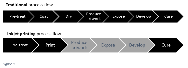
Advantages of Inkjet Soldermask Process The inkjet process offers many benefits to both the PCB producer and end user when compared to the LPISM process (Fig 8)..
Reduction in process steps The inkjet process offers a reduction in process steps compared to the LPISM process, by eliminating the coating, artwork preparation, exposure and development steps, resulting in large energy savings from the elimination of the drying ovens and high-power UV exposure equipment. The reduced number of process steps also results in reduced WIP and a gain of reusable space in the PCB plant. Digital “artwork” Ink jet printing is a digital process and the print pattern is created straight from Gerber data or via a bit-map, thus eliminating the artwork preparation process and freeing up storage space used to store artworks. It also means changes to the artwork can be made quickly and easily and enables dynamic data information such as sequential numbering to be used. Potential for high throughput The potential for a high throughput printing process depends on number of heads, droplet size, frequency of operation and print strategy. The ideal objective for printer integrators is to enable single pass printing by using enough heads to span the width (or length) of the boards to be printed. However, the print strategy used may affect this, if it requires multilayer printing to achieve the required image quality. Additive process As a direct image process, putting the soldermask only where it is required and with selective thickness control, there is minimal wastage of material. Consideration has also been given to copper only printing where the soldermask is applied only over the actual circuitry Low/no solvent emissions UV curing inkjet soldermask have relatively low amounts of volatiles emitted during processing. Compare this to a PCB plant using about 150 kg/mth LPI ≡ 630kg/year solvent emitted.
Registration compensation/image stretching and offset to allow for board distortion The digital artwork permits adjustments to be made locally, and overall, in the x and y to compensate for board and image distortion and to achieve good registration. Reliability Ink jet printing itself is a very repeatable process and should require little user intervention once set up correctly. Furthermore, the soldermask materials are 100% solids and minimise the amount of material used to achieve a given thickness. Unlike photoimageable soldermasks, the image created by inkjet printing has no undercut at image edges, eliminating the possibility of trapped chemistry which later causes corrosion and/or adhesion loss.
Strategies for Print Optimization In order to achieve the required image quality printers may use a number of different print strategies. The first of these, already discussed, is pin-curing. An integral UV LED light source effectively cure the jetted soldermask moments after it lands on the substrate, limiting the opportunity for the ink to flow out because of the low viscosity. Multilayer print profiles can also be used whereby, the soldermask coating is built up in layers by printing “dams” around image edges before printing the rest of the board, or selectively along the sides of tracks to improve coverage on track edges.
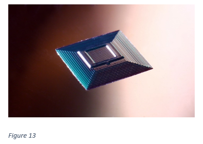
Using this kind of approach, also makes it possible to build 3D type structures such as the pyramid type structure in Fig13 which is over 200 microns high.
Electrajet ® EMJ110 - Performance, properties and comparison with LPI soldermask Detailed below are tables of the performance test results achieved to date with Electrajet® EMJ110 Ink Soldermask
Conclusion These results demonstrate that development protocol above, combined with years of formulating experience and product knowledge have resulted in ElectraJet® EMJ110 Inkjet Soldermask, a fully functional Inkjet Soldermask capable of meeting industry and OEM requirements. |
||||||||||||||||||||||||||||||||||||||||||||||||||||||||||||||||||||||||||||||||||||||||||||||||||||||||||||
| Go back to Contents | ||||||||||||||||||||||||||||||||||||||||||||||||||||||||||||||||||||||||||||||||||||||||||||||||||||||||||||
| Section 9 |
PCB Fabricators Group - a Benefit to all who Fabricate PCB’s in the UK. |
|
Steve Lloyd Chairman of the PCB Fabricators Group |
An update will appear in the next issue |
| Section 10 |
Industry News |
| 10.1 |
Stevenage Circuits
Trackwise acquires Stevenage Circuits: |
| 10.2 |
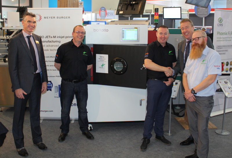
Adeon Technologies Merlin Flex Ltd, part of the Merlin Circuit Technology Group in the UK orders a Boffotto P06H PCB Plasma processing system during Productronica 2019. The system will be delivered before the end of the year. The P06H will increase further the specialised treatment of the high-tech Flex PCB's that Merlin manufacters in its Hartlepool UK site.
|
| 10.3 |
Eurotech Group UK PCB manufacturer The EuroTech Group have announced the acquisition of Lyncolec, based in Poole, Dorset. The deal will see the enhancement of EuroTech’s manufacturing capability to include Flex and Flex Rigid PCBs, this complements its current offering and will...Read more |
| 10.4 |
Exception PCB On Wednesday 11th March Exception PCB put on their Kit to participate in a 5-a-side Football game to raise money for Sports Relief. With a few short, Lisa Trust who works in Production Control stepped up and agreed to be in goal instead of being a supporter. Technical Sales Director, Mike Devine got his ref kit on to ensure things were fair even if his head height did change throughout....
|
| 10.5 |
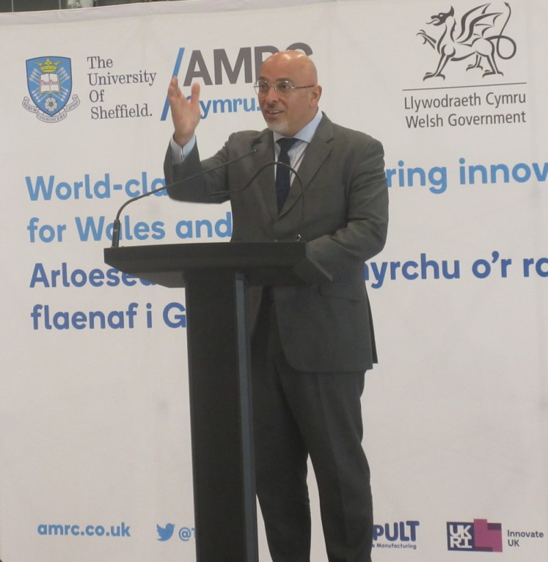
Merlin PCB Group Merlin Meets MP Nadhim Zahawi 18/02/2020 Merlin Meets MP Nadhim Zahawi Parliamentary Under Secretary of State (Minister for Business and Industry) The Aerospace Growth partnership invited Merlin Circuit Technology and other businesses to represent Welsh Aerospace industries at the Advanced Manufacturing and Research Centre (AMRC) unit set up in collaboration with Airbus, The Department for Business
|
| 10.6 |
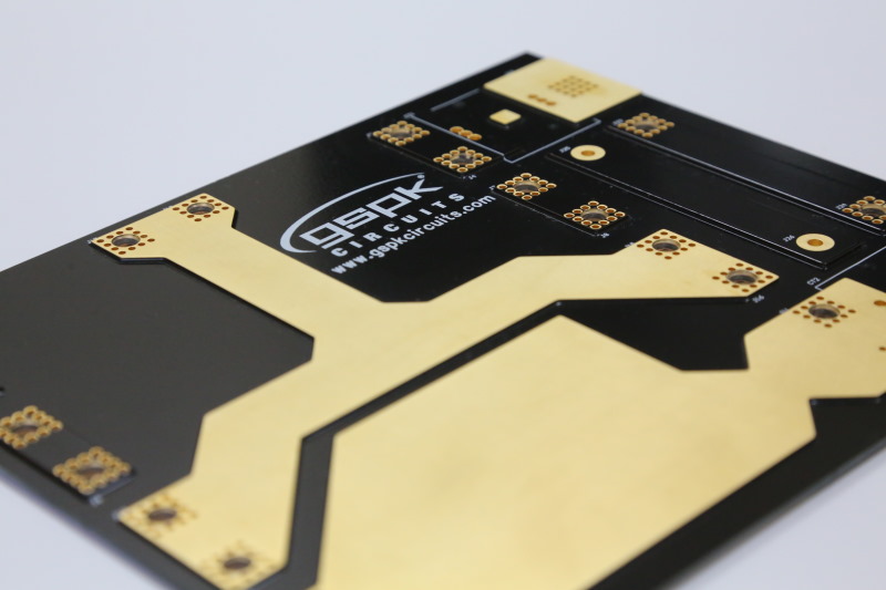
GSPK (TCL Group) GSPK Now Supplying Heavy Copper PCB’s On top of our comprehensive PCB and IMS capability, GSPK Circuits are now supplying Heavy and Extreme Heavy Copper PCB’s. An increasing number of power electronics products are taking advantage of a growing trend in the printed circuit board industry: Heavy Copper and Extreme Copper Printed Circuit Boards.
|
| 10.7 |
Amphenol-Invotec Ltd An interview with Jeremy Brook - discussing Invotec's growth in the Space sector A. The Space sector is certainly significant for us and fits very well with our scope of being recognized for supplying complex, high performance PCBs to high reliability markets that also includes Aerospace & Defence, Communications, Automotive, Rail and Power industries. Sales to the Space sector now represent greater than 10% of our turnover. To look at it another way, we have supplied product to over 50 different global customers.
|
| 10.8 |
Ventec Europe We are delighted to announce the appointment of Leigh Allinson as Technical Sales Manager to offer key technical and sales support to customers in the United Kingdom. Leigh will be taking over the technical support aspects of his responsibilities from Ian Mayoh who will be semi-retiring and focusing on specialist client projects after 11 years in his role as Technical Support Manager.
|
| 10.9 |
Zot Engineering Ltd Zot Printed Circuits are pleased to announce that they have placed an order for a new Schmoll MDI - supplied and installed by Schmoll Maschinen GmbH. The new digital imaging system increases capability and capacity for processing high technology, high reliability Printed Circuits. The equipment is part of ongoing investment in the PCB facility, so we can give our customers the highest quality and best service at all times..
|
| Go back to Contents |


|
Section 11 Corporate Members of The Institute of Circuit Technology September 2018 |
||
| Adeon Technologies BV |
Weidehek 26,A1 4824 AS Breda,The Netherlands |
www.adeon.nl |
| Atotech UK Ltd. | William Street, West Bromwich. B70 0BE | www.atotech.com |
| CCE Europe | Wharton Ind. Est., Nat Lane, Winsford, CW7 3BS | www.ccee.co.uk |
| ECS Circuits Ltd. | Unit B7, Centrepoint Business Park, Oak Road, Dublin 12, Ireland | www.ecscircuits.com |
| Electra Polymers Ltd. | Roughway Mill, Dunks Green, Tonbridge, TN11 9SG | www.electrapolymers.com |
| The Eurotech Group | Salterton Industrial Estate, Salterton Road, Exmouth EX8 4RZ | www.eurotech-group.co.uk |
| Exception PCB Solutions | Ashchurch Business Centre, Alexandra Way, Tewkesbury, Gloucestershire. GL20 8NB | www.exceptionpcbsolutions.com |
| Merlin PCB Group | Hawarden Industrial Park, Manor Ln, Deeside, Flintshire, North Wales, CH5 3QZ | www.merlinpcbgroup.com |
| Faraday Printed Circuits Ltd | 15-19 Faraday Close, Pattinson North Ind. Est., Washington. NE38 8QJ | www.faraday-circuits.co.uk |
| Graphic plc | Down End, Lords Meadow Ind. Est.,Crediton EX17 1HN | www.graphic.plc.uk |
| GSPK (TCL Group) | Knaresborough Technology Park, Manse Lane, Knaresborough HG5 8LF | www.gspkcircuits.ltd.uk |
| Amphenol Invotec Ltd | Hedging Lane, Dosthill, Tamworth B77 5HH | amphenol-invotec.com |
|
HMGCC |
Park Rd, Milton Keynes MK19 7BH |
|
| Holders Technology UK | Tweedbank Industrial Estate, Tweedbank, Galashiels TD1 3RS | ww2.holderstechnology.com |
|
Minnitron Ltd |
20 Leigh Road, Haine Industrial Park, Ramsgate, Kent CT12 5EU |
|
| PMD (UK) Ltd. | Broad Lane,Broad Lane,Coventry CV5 7AY | www.pmdgroup.co.uk |
| Rainbow Technology Systems | 40 Kelvin Avenue, Hillington Park, Glasgow G52 4LT | www.rainbow-technology.com |
| Stevenage Circuits Ltd | Caxton Way, Stevenage. SG1 2DF | www.stevenagecircuits.co.uk |
| Sun Chemical | Norton Hill, Midsomer Norton, Bath | www.sunchemical.com |
|
Teledyne Labtech |
Broadaxe Business Park, Presteigne LD8 2UH |
|
| Ventec Europe | 1 Trojan Business Centre, Tachbrook Park Estate, Leamington Spa CV34 6RH | www.ventec-europe.com |
| Zot Engineering Ltd | Inveresk Industrial Park Musselburgh, B19EH21 7UQ | www.zot.co.uk |
| Go back to Contents | ||
| Section 12 |
Editors Notes The ICT Journal |
|
Instructions/hints for Contributors 1. As it is a digital format the length is not an issue. Short is better than none at all! 2. Article can be a paper or a text version of a seminar or company presentation. Please include data tables, graphs, or powerpoint slides.We can shrink them down to about quarter of a page. Obviously not just bullet points to speak from. 3. Photo's are welcome. 4. We would not need source cross references 5. Title of presentation - Of course! Date, Job title of Author and Company represented. 6. An introductory summary of about 150 words would give the reader a flavour of what it's all about. 7. Style - we don't want out and out advertising but we do recognise that the speaker has a specialism in the product or process that will include some trade promotion. Sometimes it will be a unique process or equipment so trade specific must be allowed. 8. Date and any info relating to where or if this article may have been published before. 9. We can accept virtually any format. Word, Powerpoint, publisher, PDF or Open Office equivalents. 10. Also, to make it easy, the author can provide a word file to go along with his original powerpoint presentation and I/we can merge it together and select the required images. 11. A photo of author or collaborators.
I really do look forward to receiving articles for publication. Lynn Houghton |