|
The Journal of |
| Section 1 | Editors Introduction |
|
Richard Wood-Roe |
In this issue of The Journal we have included 3 interesting papers. The first 2 are linked to the subject of the skin effect of conductors and how the finish and surface roughness affect the signal integrity. The first paper is an assessment of Surface Finish on the performance of high frequency PCB's from MacDermid Alpha Electronics Solutions. The second describes a process of Photoresist Adhesion enhancement while maintaining minimal surface roughness from Atotech. Finally the third paper, from Pillarhouse International, reviews the challenges encountered when selective soldering PCB's. There is growth in the uptake of this manufacturing procedure and the Selective Soldering Academy has been formed to help manufacturers meet the demands of this complex process. Pete Starkey has provided an excellent review of our recent Annual Symposium. The Annual Foundation Course is also featured and is one of our key contributions to the PCB industry. The 4 day residential program provides an unrivalled opportunity to glean knowledge and expertise from some of the respected leaders in our manufacturing and supplier companies. This is an excellent project and will provide continuity of skills and expertise to new blood in our industry. We sadly report the passing of two of our fellow members, Martin Cotton and Norman Fergusson. Finally the industry news section highlights the activity of some of our Corporate Members. I hope you find the contents of the Journal interesting. I welcome your feedback. |
| Go back to Contents |
| Section 2 | Calendar of Events | |
Bill Wilkie |
2023 |
Details |
| September |
September Wednesday Webinars 6th September: Ventec International, CT Engineering and Polar Instruments 13th September: Isola and Viking 20th September: CCI Eurolam, Adeon and A-Gas 27th September: Peplertech |
|
| December 5th |
Christmas Seminar Sponsored by local companies: Faraday Circuits, Fineline VAR and GSPK Circuits. |
|
| Go back to Contents | ||
| Section 3 |
Reassessing Surface Finish Performance for Next Generation Technology - Part 1 |
|
|
Introduction As system designers continue to respond to new performance demands, it can be noted that ENIG/ENEPIG finishes have endured as a leading choice in many advanced applications where reliability is prioritized over cost. Electroless nickel (EN) deposits have served well as a barrier layer preventing copper migration to the outer gold or palladium-gold surfaces, enabling the robust solderability performance of ENIG and ENEPIG finishes. However, the introduction of the 5G mobile network creates a growing demand for smartphones, networking, and wireless connections, all requiring increased “data flow” The need to reduce the signal loss at higher frequency bandwidth is becoming vitally important. The low conductivity and magnetic properties of EN affect electrical signals as they travel along the conductor’s outer surfaces leading to insertion losses at higher frequencies. As a result, designers and fabricators are looking for newer-generation surface finishes to meet their performance criteria. EPIG (Electroless Palladium and Gold with no EN), Silver-Gold (Ag-Au), as well as reducing the EN thickness from traditional ENEPIG, have all gained attention. This paper reviews and compares the performance attributes of the leading candidates for a high-frequency alternative surface finish. MacDermid Alpha Electronic Solutions has worked in partnership with Rogers Corporation to evaluate the effect of various surface finishes on signal loss with increasing frequency. Together, we subsequently worked to understand, and compare other critical-to-quality performance metrics that will guide application-based surface finish selection. • Standard ENEPIG (4µm Electroless Nickel / 0.1µm Palladium / 0.05 µm Gold) Following the evaluation of insertion losses, each surface finish was assessed based on other performance criteria: • High Speed Ball Shear After data collection, it was summarized, and a decision matrix was constructed to allow designers to compare performance requirements against each surface finish’s capabilities. Insertion Loss Testing αT=αD+αC+αR+αL (1) where αD, αC, αR, and αL represent the dielectric loss, the conductor loss, the radiation loss, and the leakage loss, respectively. If the transmission line is an ideal impedance matching circuit, the total transmission loss can be expressed using only two dominant factors, i.e., the conductor and dielectric losses, as shown in Equation 2 [1] αT=αD+αC (2) Multiple factors affect the conductor loss of the transmission line including surface roughness of the Copper foil, skin effect, and magnetic permeability of the conductor. The skin effect is closely related to the surface finishes. When the frequency of the signal increases, the current flowing in the transmission line focuses on the surface of the Copper foil, instead of the center of the foil. This is known as the skin effect. The skin depth δ - amplitude of the current flowing on the surface of the transmission line can be derived using Equation 3 below [2,3].
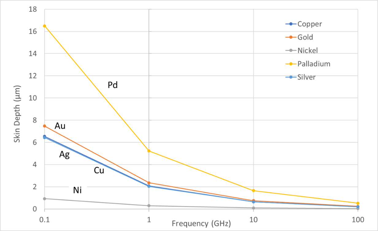
Figure 1 shows the skin depth of Copper (Cu) and the plating material of fabricated transmission lines [4]. The results demonstrate that Pd had the deepest skin depth. Followed by Gold (Au), Silver (Ag), Copper (Cu), and Nickel (Ni). Ni, which is ferromagnetic, with the highest magnetic permeability, and has a shallow skin depth, whereas a low electrical conductivity, Pd, has improved skin depth. At 1 GHz, the skin depth of Ni is less than 0.5 µm. Figure 1: Skin depth in Cu and other plated finishes
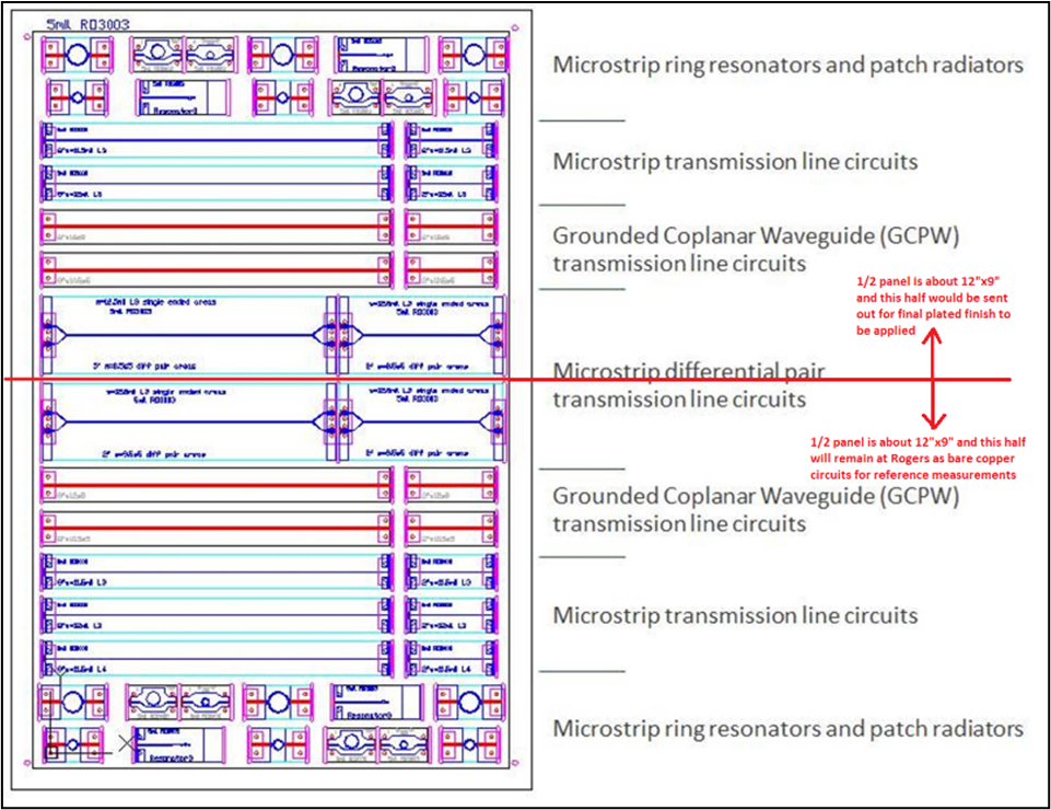
Figure 2: Rogers signal loss test of a vehicle consisting of identical top and bottom halves
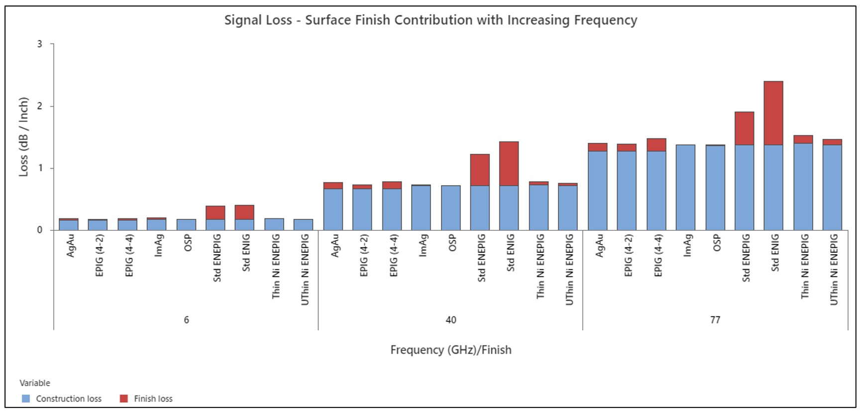
• 6 GHz – standard operation The stacked bar includes two components. First, the blue bar represents loss due to the construction of the test vehicle (the data obtained using the copper only half of the test vehicle). Second, the red bar showing the additional loss due surface finish application to the second half of the same test vehicle. Figure 3; Signal loss due to construction (blue) and surface finishes (red) at representative frequencies
Insertion Loss Data Analysis In a perfect world, we would hope to observe the same signal loss from each of the copper-only test vehicles. However, experimental errors are possible reducing repeatability between tests. The variance observed between the construction-only losses is believed to be due to either signal loss measurement error or more likely minor differences in the construction (etched definition, trace uniformity, surface roughness, etc.) between the individual test vehicles. These differences are small enough to allow effective judgment and comparison of signal losses for each surface finish. Once taking into consideration the minor experimental variance, it is possible to categorize the surface finish test candidates into three categories: Category One: Category Two: Category Three: Conclusions The new generation surface finishes (Ag-Au, Thin EN ENEPIG, and EPIG) continue to outperform traditional ENIG and ENEPIG. Other selection criteria, such as environmental resistance, soldering performance, solder joint reliability, and wire bonding, make these newer finishes attractive for certain applications where OSP and Silver cannot meet performance needs. In the upcoming Part 2 article, a data driven review, examination and comparison will be presented on High Speed Ballshear, Drop Shock, Wirebonding, and Solder Joint reliability performance of the newer generation and traditional surface finishes. A decision matrix will be included to assist designers in aligning performance needs with surface finishes capabilities. References: |
| Go back to Contents |
 Frank Xu
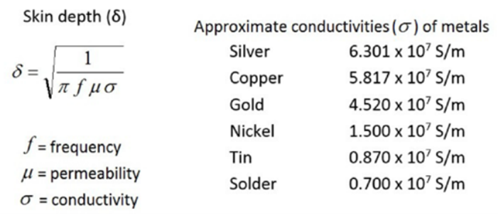
| Section 4 |
Nano Structuring Photoresist Adhesion Promoter Christopher A. Seidemann, Thomas Thomas, Fabian Michalik, Patrick Brooks, Wonjin Cho. Atotech Deutschland GmbH |
|
Chris Seidemann |
1. Abstract In order to approximate this objective, it is essential that noise, distortion and losses of data signals are significantly reduced, since these parameters represent the controllable framework conditions of a telecommunication device, which are directly related to performance losses in terms of transmission speed, reception range and latency. However, common adhesion promoters used in several process steps in the manufacturing of classical PCBs, MLBs and HDI circuit boards are to some extent causing these problems due to the nature of their work mechanism – surface roughening. While these effects played a negligible role at lower frequencies, they now take center stage as distortion, losses and noise amplify with an increasing frequency and roughness. As a solution to this problem, the industry is primarily focused and eager to develop new dielectric materials and non-etching adhesion promoters for inner layer bonding applications. However, further opportunities exist in other production steps, where the signal integrity can still be improved by displacing commonly used micro-etching surface pretreatments for solder-mask and photoresist adhesion with low or non-etching alternatives. Unfortunately, this leads to a subsequent problem, namely lower adhesion, and low production yield due to a weaker mechanical bond. This work describes the functional principle of a novel, anisotropic, nano-copper engraving, photoresist pre-treatment for multilayer and advanced HDI PCBs. It is designed to optimize the signal integrity especially for high frequency applications, while ensuring excellent adhesion. This is done by a two-step surface treatment process, which involves an ordinary cleaner to remove mild oxidation and a special anisotropic conditioner, which selectively engraves nano cavities in z-direction, while maintaining the integrity of the surface dimension. The data indicates that this method can in fact combine the benefits of classical micro-etching and newer non-etching solutions and seems to be a viable addition to the high frequency PCB production process. For decades the answer to ensure temporary as well as permanent adhesion of copper surface to a series of base and photoresist materials was to increase the roughness of the metal surface by wet chemical etching processes. Nowadays the situation tends to change and the driver for this development is among others mainly the new 5G mobile communication standard and hence new limitations for the roughening processes during PCB manufacturing. It is known that with increasing frequency, the so-called "skin effect" intensifies, which states that direct current tends to flow along the outer walls of a conductor track. If the effect increases, the area of the conductor used shrinks further and the current flows proportionally more on the roughened outer surfaces. This in turn leads to an increase in the distance the current must flow, which is the main driver for an increase in signal loss. To counteract this effect, the market trend, especially for permanent adhesion, is tending more and more towards low-roughening processes. Manufacturers, however, focus primarily on permanent adhesion with regards to low roughening treatments. The obvious reason for this is, that only the final roughness, created in the last step when designing the conductor track, defines all signal integrity properties. With immense effort, a lot of progress was reached in order to minimize the roughening either by reducing etch depth, adding chemical adhesion promotor, or finetuning processes towards lower surface roughening for this purpose. However, one process step during advanced HDI manufacturing was neglected for a long time in terms of minimizing the overall conductor roughness - This was processes for temporary adhesion. During manufacturing, the core CCL layer will be structured by classical Develop Etch Strip (DES) technique and typical photoresist pre-treatments for this approach lead to SA values of ~300 nm and to ST values even greater than 2 µm. Considering nano or non-roughening adhesion promotors in the final production step, the surface topography established during the resist pre-treatment likely will influence the overall roughness. Therefore, one should not only be aware of the final permanent adhesion treatment but also consider other processes during the conductor build up to further optimize the signal integrity. 3.Material and Methods 3.a Process flow
Figure 1: Schematic LRDFP process flow (top) and typical surfaces topography before and after etching on e-less and DC-Copper (bottom). The function of each individual step of the process is described in the following: LRDFP Conditioner is a metal surface conditioner that modifies the surface morphology without noticeably reducing the copper layer thickness (few nanometres). In this step copper is removed unequally in depth with a proven etch depth working window of 50 nm up to a maximum of 200 nm (measured by weight loss). Since the selective etching is a novel technique that differs substantially from classical etching procedures a more appropriate term that describes the surface modification more precise should be used – nano structuring. 3.b Surface characterization setting 3.c Evaluation of photoresist adhesion performance
Figure 2: Top: schematic surface modification by DES Pre-treatment followed by modifications of bonding processes. Bottom: FE-SEM images after each surface step at the same magnification. With low roughening and especially low etching surface modifications in the adhesion enhancement step, main roughening issues will be shifted to the upstream processes. Hence DES pre-treatment should be a critical part in the whole signal integrity improvement plan. To gain understanding on the influence of DES pre-treatment on overall roughness several pre-treatments in combination with ultra (low) roughness bonding processes for 5G were evaluated on its critical point with regards to surface roughness (Figure 3).
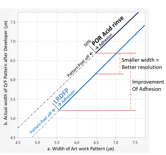
In Figure 3, one can see the influence of DES-coating on the overall surface roughness by FE-SEM. Especially for low roughening and less etch depth processes in the 5G bonding step, the influence of DES pre-treatment cannot be neglected. It appears to be predominant for the overall surface roughening and hence for the signal integrity loss. A deep random orientation of crater can be already seen for sample treated with conventional DES pre-treatment (CuCl 0.5 and 1.2 µm), resulted in high initial surface roughness. Thus, further treating surface with 5G bonding step would further increase the surface roughness. Meanwhile, LRDFP treated sample shows a relatively shallow crater, and further treatment with 5G bonding has no significant effect on crater steepness. This can be also confirmed by the roughening values obtained after different combinations of DES- and 5G-bonding treatments (Figure 4). The value of RSAI (%) represents the degree of surface roughness, with rougher surface for higher value. The measured RSAI(%) of LRDFP treated sample shows the lowest value among other pre-treatments even after 5G bonding treatment. Figure 4: Roughness values for combinations of DES-pre-treatments with 5G bonding treatment measured by Laser Confocal Microscope. Based on the above result, it could be proven that a DES process that yields a lower roughness in its treatment steps correlates with the overall roughness after a 5G bonding treatment and hence low roughening adhesion enhancement process for temporary adhesion must be included for optimization of signal integrity loss. Consequently, DES roughening must be optimized to obtain the best possible 5G signal results while ensuring the necessary adhesion to not lose any temporary adhesion performance. LRDFP, as indicated by the data, seems to be a viable option to fill this gap and provides ultra-low surface roughening. This combines with excellent resist adhesion properties proved by line width observations with settings that normally only apply for (advanced modified semi additive processing) MSAP and SAP applications. Hence, were tested by a higher standard than necessary. 5. Adhesion Results Figure 5: Top: fluorescence microscopy images for lines with 50 µm space. By fluorescence microscope one can see that line adhesion significantly improved due to the use of LRDFP. Furthermore, an advantage of 1.15 µm of the 50% adhesion value resulted compared to the Post Oxide Removal (POR) (acid rinse). Only a slight impact of the etch depth for LRDFP adhesion values occurred which confirmed a broad working window of 50-150 nm etch depth. A key for reliable adhesion is the connection at the resist/copper interface. Only a reliable connection ensures plating performance and even conductor shapes. Due to the microroughened surface structure and high RSAI values for LRDFP, good wetting and a reliable interfacial connection even for prolonged developing time is provided (Figure 6). Beside adhesion, resolution is as well a key feature for temporary adhesive coatings. It turns out that resolution for one-to one L/S ratio of resist lines were affected by the etch depth of LRDFP. Based on the micro-roughened surface the (back)scattering of light during exposure is hindered and LRDFP acts to some extent as an antireflective coating. Consequently, the line width for a given UV exposure energy is reduced and hence the resolution can be improved (Figure 7). Figure 7: Fluorescence Microscope images to determine resolution for L/S = 4/4, 6/6 and 8/8. Due to the anti-reflective coating properties the resolution can be increased up to 2 µm compared to the acid rinse treatment and hence finer features can be obtained. In Figure 8, the advantages of LRDFP in terms of adhesion and resolution against POR are summarized. Applying this process, an adhesion increase of > 1 µm for isolated features can be obtained in combination with a higher resolution due to the beneficial anti reflective surface properties. In combination with the minimal impact on the signal integrity loss due to the low etch depth and (ultra-) low roughening properties, LRDFP fulfils all needs of a photoresist pre-treatment for multilayer and advanced HDI PCBs. In combination with other low roughening adhesion promotor processes, it can be used to ensure minimal signal integrity loss and exploit the full potential of 5G communication technologies. Looking at the influence of different dry film pretreatments on the final roughness of a PCB surface, it was found that a focus only on low etching bonding process is not sufficient to obtain optimal signal integrity results. When using an adhesion promoter specially designed for high-frequency applications, it was possible to show that the overall roughness as measured in RSAI was reduced by approximately 30% only by using LRDFP dry film pretreatment in a prior production step. It also became apparent that a nano-etching dry film pretreatment has positive effects on the overall roughness even when a high etching adhesion promoter was used, contrary to initial assumptions. The goal around the overall process of trace and in general PCB manufacturing must therefore be to pay attention to all manufacturing processes, from start to finish. Unfortunately, it was not possible at this stage to prove signal integrity improvements by measuring the SI loss. One can, however, confidently assume that there should be an improvement by decreasing the overall roughness, since the influence of the skin effect is well researched and often verified. In order to obtain greater certainty about the results just presented, it would be of great interest to repeat such an inquiry using a dedicated signal integrity measurement method while using various high frequencies to see the magnitude such an improvement would bring for each frequency. Furthermore, the adhesion tests showed that a shallow etch depth does not necessarily have to lead to poor adhesion or reduced resolution. Rather, the LRDFP process could be used both in case of high frequency applications for HDI-PCBs and in terms of resolution gains for mSAP and SAP as well. This in turn implies that such a pre-treatment solution could be used for a wide variety of purposes and could yield different benefit for each of them. “This paper was first presented at ©2022 IPC APEX EXPO Technical Conference, with original work published within conference proceedings.” |
| Go back to Contents |
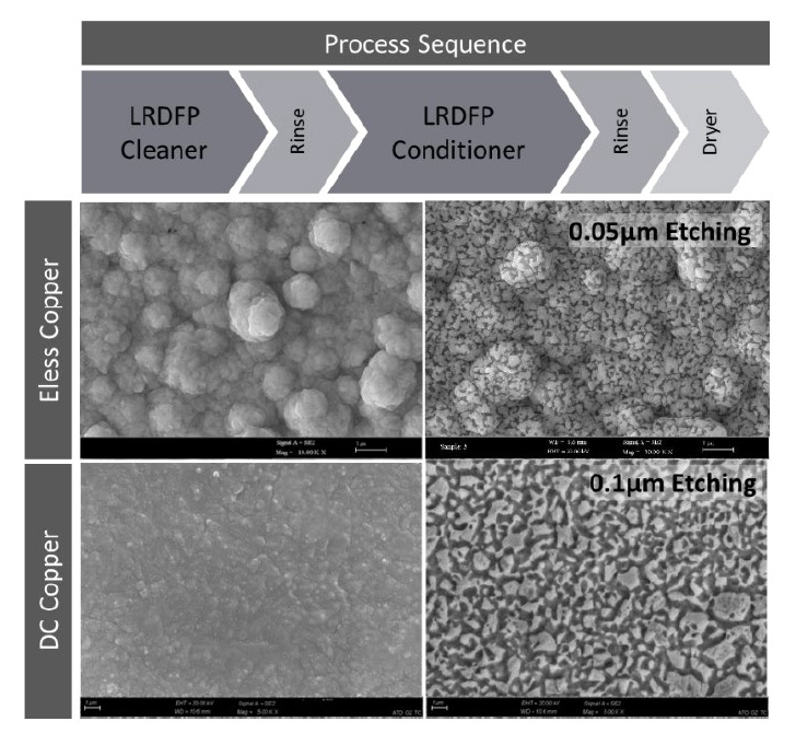
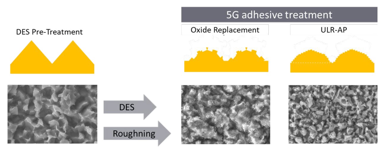
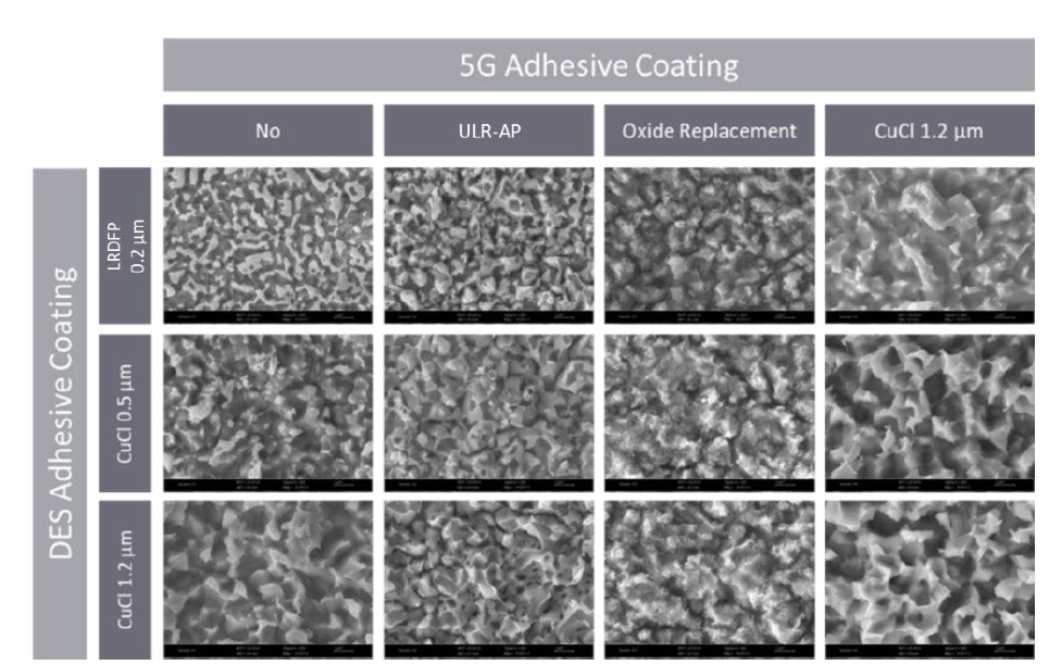 Figure 3: FE-SEM images for combinations of DES-pre-treatments with 5G bonding treatment.
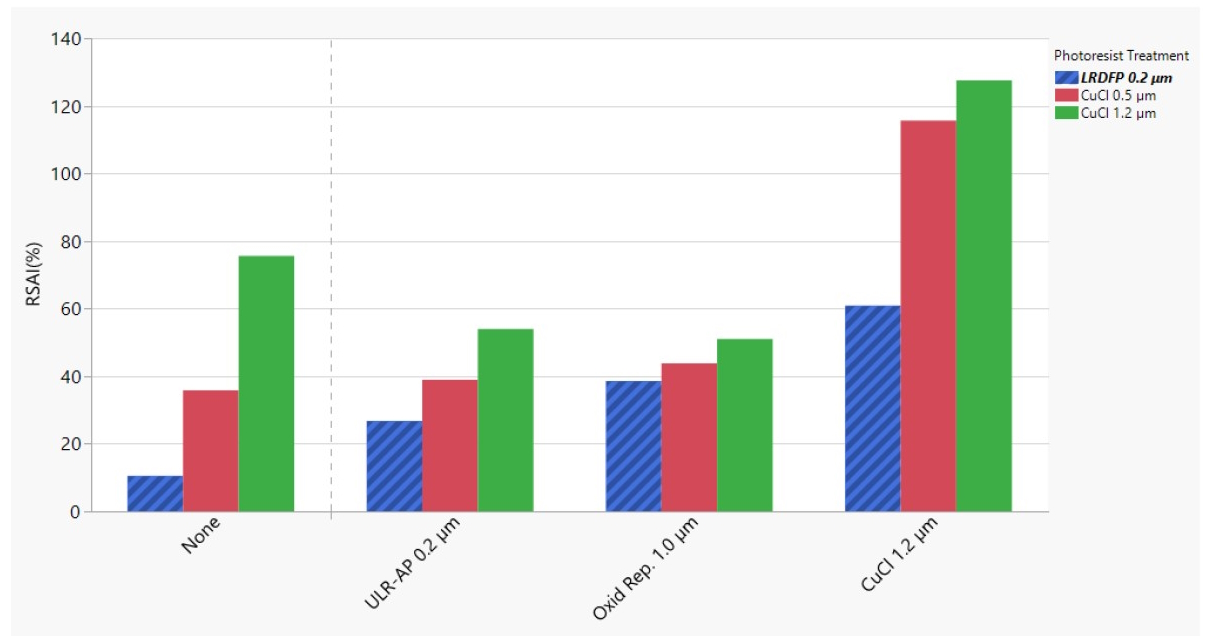
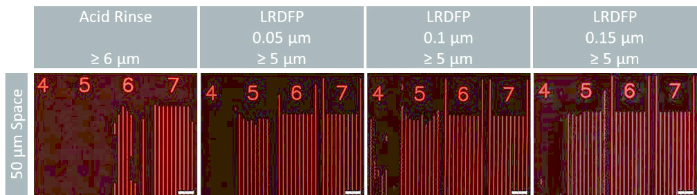
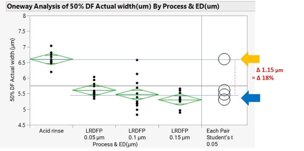
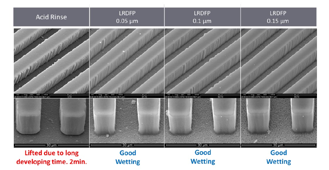 Figure 6: Street-view FE-SEM images of photoresist lines and the connection of Cu/resist interface for L/S = 10/10 µm.
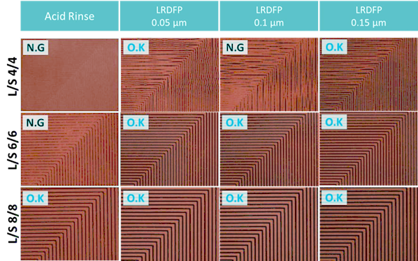
| Section 5 |
The Challenges in Selective Soldering and Meeting Training Needs Samuel J. McMaster*1,2, Kane F. Witham1, Andrew Cobley2, John E. Graves2, Eddie Groves3 |
| 1. Introduction
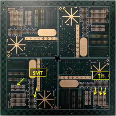
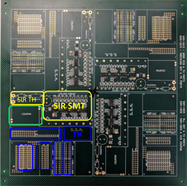
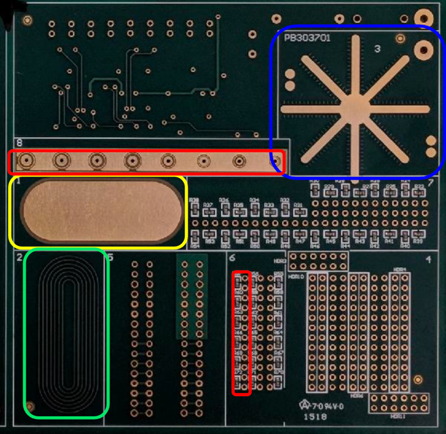
Selective soldering has grown in popularity over the past 25 years to now be a major connective technology in the electronics industry. The machines and techniques have progressed to being a major feature of in-line processes with the ability to flux, pre-heat and solder through-hole technology (THT) components for printed circuit boards (PCBs) within a single machine or series of modular machines. As described by McMaster et al. [1], there are 2 classes of selective soldering machines: hand-load and in-line machines. As in-line systems are used for processing either a greater volume of boards or larger boards, many of the most challenging selective soldering processes are undertaken with this equipment. 2. Challenges in selective soldering 2.1. Process challenges • Creating a film between the solder mask and the solder to avoid the adherence of solder to the PCB. There is no one size fits all flux; they can be alcohol-based, water-based or rosin based. Solid content can vary as can the active chemistry. Application methods can vary depending upon the process requirements but generally, two methods are used. The drop-jet can quickly apply miniature droplets in a precise fashion. Water and alcohol-based fluxes can be used with the drop-jet. When a larger area is to be soldered, an ultrasonic head is used. This fluxing module is lower maintenance and can handle higher solids content fluxes. After fluxing, the board would generally be pre-heated. This activates the chemistry and prepares the board to better wet the applied solder. Most commonly, infrared (IR) lamps are used with a wavelength between 750 nm and 3000 nm. Balancing the wavelength of the IR with the absorption of heat of the parts is key. IR can quickly respond (1-3 seconds) to heat the board and can be used in closed loop mode (taking a temperature reading and altering the power to hit a desired thermal profile) or open loop (where the lamps simply heat the assembly without imposed power control) For thicker boards, convection heating may be used. This technology is slower to respond than IR resulting in pre-heating steps in the range of multiple minutes compared to 1-2 minutes for IR. Convection is, however, able to evenly heat thicker PCBs and isn’t bound by the reflectivity issue of different wavelengths of IR lamps. To achieve the optimal pre-heating for a specific product, a thermal profiler should be used to determine the maximum temperature, thermal ramp rate and pre-heating time. For some processes, the PCB is then enough that pre-heating doesn’t need to be used and the heating from the applied solder is enough. The order of fluxing and pre-heating can be changed depending on the process requirements for the board and depending upon the flux being used. As heating is applied to the board, a water-based flux will spread whereas an alcohol-based flux will begin to evaporate. Proper process engineering ensures that the order and timings of these processes are specified. Following these steps, it’s finally time for soldering. As with all the other elements of the selective process, there are multiple parameters and options to consider during this step: • Inertion: To maintain good flow characteristics and reduce the amount of bridging, a low-oxygen environment is used. Nitrogen is typically used for inertion to achieve sub 10 ppm of oxygen. 50 ppm of oxygen is the maximum permissible limit, above this the solder quality is affected and dross is generated at a higher rate. • Positioning of the solder bath : The bath positioning can be used to either apply soldering to a single joint or closely packed series of joints in a dip step or movement along the underside of a PCB. The machine can be programmed for rows of connectors as part of a draw step. • Contact time of solder: Greater contact time can aid wetting and pull-through of solder but increasing the time can dissolve copper from the PCB. • Type of solder: lead-free or leaded; inclusion of additives to alter the liquid properties or the mechanical properties of the solidified joint. • Use of wetting or non-wetting nozzles: non-wetting dip nozzles can be used for fast production of high-volume products, but they lose the per-joint customisation of a wetting nozzle. • Top-side heating during soldering: used if the assembly has a high thermal mass that required continuous heating to ensure good solder pull-through. • Solder temperature: The soldering temperature is chosen to balance good pull-through, flux activation loss and increased likelihood of oxidation. Generally, the temperature will be in the range of 280-320 °C. • Board warp correction: the application of heat to the PCB can warp it enough to affect the soldering process. The use of a laser positioning sensor can apply live offsets to the programmed height to achieve good soldering. Nozzle size and type can be customised for specific joints but their correct programming must still be utilised as there are so many parameters that interact to produce a well-soldered joint. With new materials engineering, the maintenance can be reduced as with the AP Master nozzles [3,4]. The increased wetting enabled by surface engineering technologies allows for faster startup of the nozzles, easier rewetting and less dewetting during process. Cleaning is still essential to keep a nozzle running well no matter the material design . A unique item that poses a challenge is not, in fact, an issue of process technology but is more people-centred. No one likes doing maintenance, but it is essential to keep all machines working properly. Machine wear out is inevitable. Proactive maintenance is undoubtedly better for a full production environment but this is more time intensive and requires greater planning [5]. Sometimes nozzle sizes are chosen to fulfil the requirements of multiple products. In this case, it is often more optimal to use planned machine downtime to swap to a different nozzle size to produce better soldering quality. This takes more time and planning from maintenance staff, however. Some customers will opt to use a heated bath trolley to allow for faster changing of baths (to use different solders or a different nozzle geometry). The heating function also allows maintenance to be carried out of the baths outside of the soldering system; when the bath cools the impeller chamber is frozen, so it is inaccessible. Finally, electronics manufacturing is becoming increasingly automated, and the soldering systems must be adapted to fully integrate with this new paradigm of manufacturing. Examples include the use of robot arms to load PCBs into the machines, resoldering in in-line soldering machines based on optical inspection results and automated nozzle conditioning and solder top-up systems. With the rapid increase in electric vehicle systems, there has been an increase in PCBs bonded to larger cooling assemblies which pose a challenge in terms of pre-heat as well as soldering larger components such as insulated-gate bipolar transistors (IGBTs). These board-specific challenges require careful setting of process parameters to ensure good soldering within the time requirements. This involves setting the pump speed to achieve the correct level of solder fill and ensuring the nozzle remains wetted, programming the optimal vectoring of the solder bath and pull-off characteristics to reduce bridging. The SSA exists to train anyone (not just those with Pillarhouse equipment) on the correct practices for running equipment, maintenance and how to approach programming new boards to enable customers to set up new processes quickly, keep them running and maximise the financial impact of the selective soldering process. The board is 0.075” (1.91 mm) thick with 4.2 oz (56.7 g) copper layers. Two of the layers are ground planes while the other two have only traces. Some connections to the ground planes are heat relieved. Silkscreen is used to partition each area of the board and each section is numbered to help identify the specific techniques to be used in each. SMT and THT are on both the board's top and bottom sides. Figure 1 shows the bottom-side of the PCB which is the starting point for THT soldering.
5. Conclusions and future developments References |
|
| Go back to Contents |
| Section 6 | ICT Annual Symposium Review June 6th 2023 |
 Bill Wilkie Bill Wilkie |
After a long crawl through heavy traffic on the M42 motorway, it was a great relief to exit at Junction 6 and arrive at the National Conference Centre for the 2023 Annual Symposium of the Institute of Circuit Technology on June 6. The conference centre is co-located with the historic National Motorcycle Museum and situated in the heart of the UK midlands, a stone’s throw from Birmingham International Airport. The delegates were welcomed by technical director Bill Wilkie. With reference to his grandson’s 5-a-side football team being instructed to “get into shape,” he commented on the changing shape of the UK PCB industry and how the Institute would continue to adapt to its geographical distribution in the choice of symposium and seminar venues. Interesting to see where we might be travelling to next year. |
|
|
The keynote presentation came from Sue and Andy Critcher, partners in a design consultancy called Total Board Solutions, with a review of the latest design requirements for board fabricators. Sue Critcher reflected upon developments in PCB design from the days of her apprenticeship, where she was hand-taping tracks and pads in the drawing office, to now using the latest design, simulation, and analysis tools, often with mixed analogue, digital, and RF technology on a single PCB. Besides the challenges of shrinking component dimensions, signal integrity, and power integrity considerations, and the increasing requirement for thermal management, project timescales are getting shorter, and the pressure is always to deliver the design more quickly at less cost. Andy Critcher reviewed some of the implications of mixed signal designs and the importance of correctly defining the stackup, particularly with the increasing complexity of RF structures. Documentation is a major concern. What data format to use: RS-274X or ODB++? RS-274X2, or even IPC-2581? He commented that not all versions of ODB++ are the same. Fabrication drawing data was another minefield, especially where the template was “copied from the last job.” Another danger area was specifications when the designer was not necessarily aware of the implications. As designers, the Critchers displayed a remarkable awareness of the challenges faced by the PCB fabricator—a consequence of spending time over many years visiting, discussing, and collaborating. Common issues with data sent from designers included drawings and specifications, annular rings too small, minimum copper spacing, clearance to pad, copper distribution and copper balancing, etch compensation, teardrops, mouse and rat bites, slivers, as well as all sorts of solder mask and silk screen issues. |
|
|
Andy Critcher spent some time discussing CAD-CAM checks, remarking, “We are checking the same thing, right?” He commented that several of the major CAD systems offer DFM capability, but remarked that although many CAD systems are available—he listed 24—each system is different. What did the future hold? As a representative of the “old guard” who had started on the drawing board and come through the ranks, learning their craft from others along the way, Sue Critcher is concerned about the current status of the PCB design industry. The world of PCB design is changing. The average age increases by a year every year and the “old guard” is moving on. A recent survey indicated that 61% of designers are aged 50 plus, only 23% are younger than 35, and 55% of designers plan to leave the profession within the next 10 years, with more than 25% retiring within five years. The “new blood” is electronics engineers from university. CAD systems continue to improve but can only take them so far. Where will these engineers get their layout knowledge and learn good practices as PCB complexity increases? The parting advice from Sue and Andy: “Talk to your fabricators!” |
|
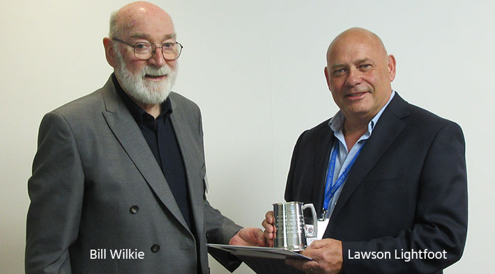
Following the Total Board Solutions keynote, Bill Wilkie took the opportunity to award certificates to new corporate and individual members, and to make a special award to Lawson Lightfoot upon his retirement from the ICT Council. Bill acknowledged the enormous contribution that Lawson had made over many years, particularly in the area of technical training and the sharing of the educational resources of the Northern UK Circuit Group. He was appointed an Honorary Fellow of the Institute.
|
|
|
|
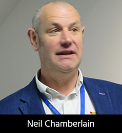
“Impedance and Beyond” was the title of the presentation of Neil Chamberlain from Polar Instruments. Referring back to “a few years ago” when he did a major house refurbishment, he learned two things: It’s important to have the right tool for the job, and to know what you’re doing with that tool. (He admitted that during his house refurbishment he had neither.) But acknowledging that within the seminar audience he was addressing designers, laminate manufacturers, and PCB fabricators, he described how Polar has always endeavoured to provide the right tools for the job and to give fabricators a coherent suite of tools for modelling impedance with a field solver, designing and documenting stackups, generating meaningful test coupons, and measuring them. “Who should design the stackup?” was a commonly asked question, whether it should be the OEM, the design guy, or the fabricator. The answer: “It depends on the customer, the requirements of the board, and the complexity of the design.” Polar has built a library of materials that covers the range that the laminators have developed over many years to fill the spectrum between standard FR-4 and Rogers 4350. It is inevitable that when a designer specifies a higher-grade, higher-performance material, someone will put a multiplier on the cost of the board. The designer must justify that cost. The library of materials allows simulations to be made with various laminates in various environments, to work out whether the material is actually required, whether standard FR-4 will give an acceptable performance, or whether the attributes of the higher-specification material are essential. All of this is specific to an individual design. Additionally, the stackup tool can generate a test coupon to enable critical parameters to be physically measured. “What loss can I expect on my system?” was another commonly asked question. “What frequency can I run this transmission line at and still get the signal I want at the other end?” Chamberlain likened a transmission line to a coaxial cable. Whatever the characteristic impedance, the longer the cable the greater the loss. Characteristic impedance is only concerned with the cross-section, not the length. However, another solver was available that could predict the losses expected along the line at a particular frequency depending on material, copper geometry, and copper roughness. Designers need to know that these methods exist and that a broad range of materials are available to avoid “taking the easy way out” and incurring the costs of over-specification. Chamberlain reviewed parameters affecting loss, discussing copper roughness and the skin effect in detail, and emphasising that at frequencies above 1 GHz the roughness of the copper could be a more important factor than the laminate itself. Therefore it was increasingly important to understand effect of the positions of “smooth” surfaces and “rough” surfaces within the stackup, and the benefits or otherwise of reverse-treated and low-profile foils. With lunch-time looming, Chamberlain’s presentation provoked much interactive discussion, involving designers, laminators, and fabricators. It was such an interesting interlude that delegates were more inclined to listen and participate than to rush off to get fed. Lunch was slightly delayed, but everyone made it back for a prompt start to the afternoon session. |
 |
Dr. Sam McMaster from Pillarhouse International discussed some of the challenges encountered in selective soldering and described how training needs are being met. Reviewing the primary elements of selective soldering, he considered options for fluxing, preheating, and soldering techniques. The drop-jet method gives very accurate flux application with minimal flux consumption and reduces the need for PCB cleaning. It can be used with water-based or alcohol-based fluxes and requires little maintenance. He demonstrated a system in action with a video clip. By comparison, ultrasonic fluxing offers rapid flux application with a high solids capability. Like drop-jet, it can be used with water-based or alcohol-based fluxes and requires minimal maintenance. Pre-heating can be done by infra-red or convection and carried out before, during, and/or after fluxing, depending on the thickness and thermal mass of the assembly and the residual activity of the flux. His video illustration showed top and bottom-side temperature monitoring. McMaster talked in detail about soldering parameters. He advocated for nitrogen inertion to maintain good flow characteristics and reduce the amount of bridging and dross generation, with 50 ppm of oxygen as an upper limit. The solder bath is positioned to apply solder to the underside of the PCB, either to a single joint by a dip step or programmed to move along rows of connectors as a series of draw steps. Longer contact times can aid wetting and pull-through of solder but can also dissolve copper from the PCB. The composition of the solder alloy determines its liquid properties and the subsequent mechanical properties of the solidified joint. Non-wetting dip nozzles can be used for fast production of high-volume products, but they lose the “per-joint” customisation facility of a wetting nozzle. Solder temperature was chosen to balance good pull-through vs. flux activation loss and the increased likelihood of oxidation. It is typically in the range of 280–320°C. Top-side heating during soldering can be used if the assembly has a high thermal mass that requires continuous heating to ensure good solder pull-through. Pillarhouse typically holds the PCB stationary during soldering, whilst moving the soldering bath and nozzle. The use of a laser positioning sensor allows live offsets to the programmed height to compensate for board warpage and achieve good soldering. Their Selective Soldering Academy provides real-world selective soldering training in troubleshooting and defect identification to IPC standards, defect examination, and elimination by control of process parameters, understanding differences in leaded and lead-free solders and surface finishes, design for manufacture with selective soldering in mind, and gaining a better understanding of machine features and their applications. |
 |
Although LED lamps may have a quoted life expectancy of 20,000 to 50,000 hours, they don’t always last that long; in reality an LED lamp will typically stop working efficiently within four to six years, degradation of the diodes will reduce the light output, and the failure of a solder joint within the assembly can result in a premature breakdown. Whatever the cause, substantial quantities of dead LED lamps are collected annually, and an essential minor component is gallium, used in the form of gallium nitride or gallium indium nitride to produce the blue component of the white-light output. Gallium is classed as a “critical raw material” meaning that it is economically and strategically important, with a high-risk associated with its supply and a lack of viable substitutes due to its unique properties. Gallium does not occur as a free element in nature, but in trace amounts in zinc and aluminium ores, and almost all of the world’s supply is produced in China. Therefore, an environmentally friendly and sustainable recovery process is easy to justify. Professor Martin Goosey from MTG Research reported the findings of the ReGail project for the recovery of gallium from end-of-life LED lamps, based on a novel, non-aqueous approach utilising deep-eutectic solvents for both gallium dissolution and subsequent electro-winning. He explained that LED chips are complex structures with the gallium typically being present as a thin epitaxially grown layer on a suitable lower-cost substrate; for example, gallium nitride is grown on silicon or silicon carbide. To gain access to the gallium, strong acids and oxidants, and high temperature thermal treatments are avoided and simple ball milling is used to produce a high surface area for subsequent dissolution with ionic liquids and eutectic solvents. Ionic liquids and eutectic solvents are environmentally low-impact, inexpensive bulk materials composed of organic cations with halide anions and an alcohol or amide complexing agent. They exhibit unusual solvation properties for metal salts and have proved useful in many materials and metal finishing applications, including electroplating. Initial work has indicated that gallium and indium can be electrodeposited from deep-eutectic solutions and that indium is deposited at a much lower cathodic potential than gallium, offering the possibility of separating the metals once they have initially been dissolved from the ball-milled granular solid. A novel method uses an electrocatalytic dissolution process with iodine as an oxidant, which is itself regenerated at the anode during the electrodeposition stage—effectively a clean, elegant, no-waste, closed-loop process. A range of deep-eutectic solvents has been investigated, and one known as Lactaline was found to be most effective. Although the original concept was to focus on gallium, most LEDs contain indium, another critical raw material, as well as possibly silver and gold. Several optimisation challenges remain, particularly regarding cost reduction and scaling-up, but the feasibility of a circular-economy approach for the supply of an important semiconductor precursor has been established. |
|
|
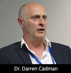
The final presentation came from Dr. Darren Cadman from the Compound Semiconductor Applications (CSA) Catapult, a government-backed not-for-profit technology and innovation centre aimed at helping the UK to become a global leader in developing and commercialising new applications for compound semiconductors through collaboration both with large companies and with start-up operations. The CSA Catapult is focused on sub-system and system optimisation and the development of tools and techniques to facilitate manufacture of product. Cadman explained that a compound semiconductor, composed of chemical elements belonging to two or more different groups in the periodic table, has unique material properties that offer many advantages over silicon, principally in terms of electron mobility, resulting in much faster processing speeds while consuming only a fraction of the energy. In power electronics and radio frequency systems, compound semiconductor devices can enable significant improvements in performance, size, weight, cost, and power. And in photonics, the distinctive emitter and detector functions of compound semiconductors provide much enhanced sensor capability. Cadman considers compound semiconductors to have the potential to drive the next wave of advances in telecommunications, robotics, renewable energy, and autonomous vehicles. Taking the telecommunications sector as an example, he stated that the Paris Agreement requires a halving of greenhouse gas emissions by 2030 and the UK had set a target of a 68% reduction from 1990 levels. He explored the benefits of an energy-efficient network in reducing carbon footprint, operational expenditure, and energy security. In a wireless cellular network, 73% of the total power consumed is associated with base stations, where power amplifiers are the dominant component with regard to power consumption, and the majority of the power used is wasted in the form of heat. The inefficiency is influenced by signals with a high peak-to-peak energy power ratio, which he illustrated graphically. The transition from 4G to 5G would require 10x more cells because of the shorter effective range of the higher frequency signals, and a shift from large central base stations to smaller local stations with power amplifiers based on gallium nitride operating at higher voltage, frequency and temperature. The CSA Catapult addresses the consequent thermal management and packaging challenges, toenhance functionality and performance while reducing cost and size. Cadman showed examples of the extensive equipment resources in its packaging facility. A further technology development he discussed was hybrid wireless bonding and interconnection of semiconductor chips using micro-bump techniques, including the UK’s first open-access, sub-10 micron hybridisation capability, together with facilities for additive manufacturing, PCB prototyping and 3D embedded packaging. |
|
In his closing comments, Bill Wilkie thanked all who had contributed, with a special mention of the table-top exhibitors, and remarked that he never ceased to be surprised at the breadth and depth of knowledge that existed within the Institute. As an additional benefit, delegates had free access to the motorcycle museum, which houses the largest collection of British motorcycles in the world with over 1,000 machines from 170 different manufacturers. A wonderful nostalgia trip to end an excellent day. |
|
| Go back to Contents |

| Section 7 |
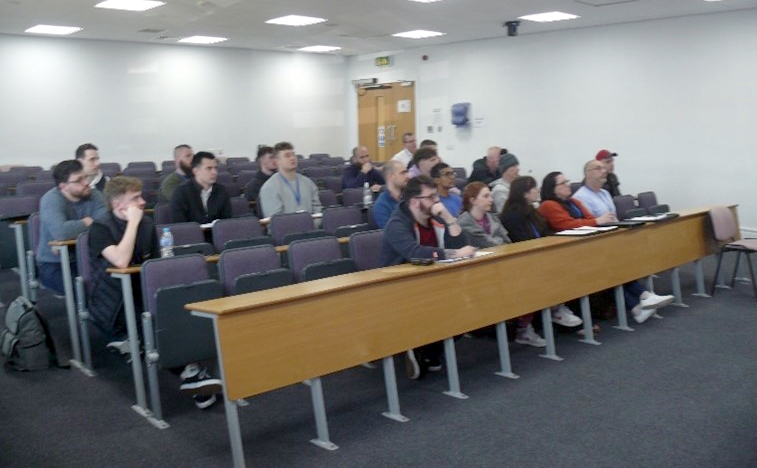
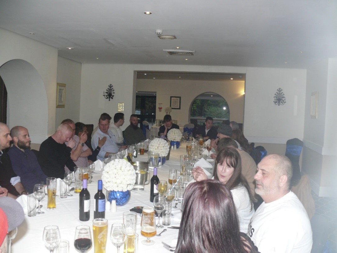
ICT Foundation Course Review April 24th - 27th 2023 |
|
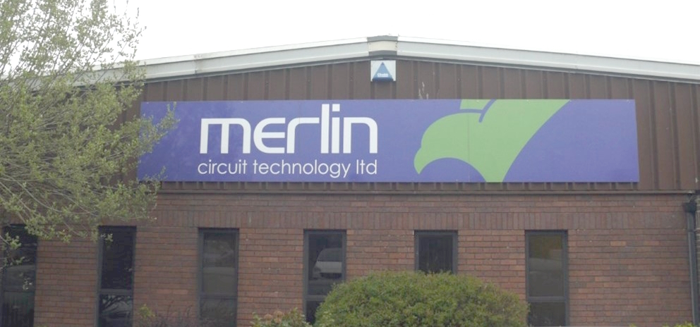
The Annual Foundation Course begins with a gentle Sunday drive down to Chester to be able to set the course up on Monday morning. The hotel is about a 10 minute drive away from the Merlin Facility at Deeside, where we hold the morning lectures and the Facility tour. Our host for the day is Mat Beadel, Technical Director of Merlin pcb and Design Lecturer for the day
2023 Delegates  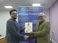 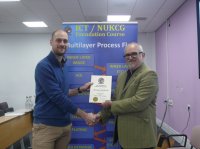 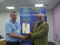 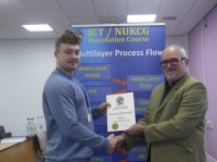     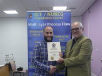 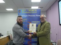 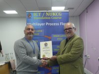 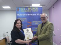         No photo: Leila Graham GSPK and Kristof Tapuska Zot Engineering
|
|
| Go back to Contents |
| Section 8 | Members News | ||
|
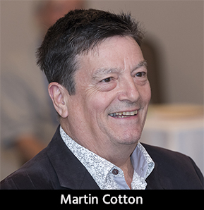
Martin Cotton |
Martin Cotton
This last weekend industry guru and dear friend to many Martin Cotton passed away. He was one of the first people I worked with in the electronics industry when I joined Toptec Design to learn to layout PCBs. He was a bit of a rockstar to many PCB designers, myself included. He was known to be among the best in his field, if not the best, and went on to be one of the most influential and innovative people in the industry over a long and distinguished career. He will be hugely missed by his family and by his numerous friends in and out of the electronics industry. Over five decades Martin performed his magic at
I spent more than forty years of my career sharing thoughts, ideas and more than a few beers with Martin. He was a mentor, a dear friend and someone I could always count on. I loved working with him and just being in his orbit, where he was the star of the show. I interviewed him on numerous occasions on camera (take a look at those interviews if you find time), and I spent many many great evenings with him just talking and laughing. He always made me think and he always made me smile.
This has also been posted to LinkedIn to encourage his numerous friends and colleagues to comment, then perhaps we can round out a tribute to this guru, this genius and this diamond geezer! Martin, we love you and we miss you! Posted by Philip Stoten May 15, 2023. Reproduced by kind permission of PCB007 Link to Article |
||
|
Norman Fergusson |
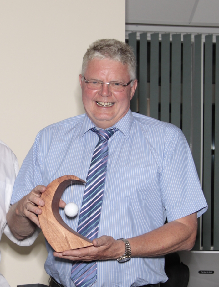
Norman Fergusson It is sad to report that Norman passed away unexpectedly in mid June. He was an active member of the ICT for many years. After leaving school Norman trained as an apprentice toolmaker. After a short time in Canada he started at Prestwick in 1974 and progressed to managing the Drilling Department. In 1987 he moved to Bodmin, Cornwall as the Production Manager for Cirbo. He later transferred into a technical sales role supporting UK customers. After 6 years he moved to Cheshire to set up the regrind and technical centre while continuing his support role in technical sales. Following the closure of Cirbo 2004/2005, Norman continued to work for the Kennametal Group which owned Cirbo and represented sister company Kemmer Prazision for some time. Since then he has spent some time working for Ventec and more recently providing technical support to the UK customers of MPK Kemmer GmbH PCB tools. This is a super photo below of one of Norman's memorable moments. Nobody wanted to win the Duffer's prize at our annual PCB golf day. Somehow Norman contrived to take 9 off the tee on one hole, so it was fitting that he was awarded this honour. As you can see he took it in good spirit.
There is a lot of camaraderie in the PCB industry and often colleagues, suppliers and competitors become good friends. There will be many of us who will have a smile in his memory and a sadness at his passing. He was always so cheerful and such a nice guy to have around and spend time with. He will be greatly missed by all of us who knew him. Link to 2009 PCB Golf Day review Richard Wood-Roe - July 2023 |
||
|
Dr. Darren Southee Loughborough University |
This is a members view of our recent symposium. A splendid Day on Tuesday June 6th 2023 at the Institute of Circuit Technology Annual Symposium which took place at the National Motorcycle Museum. The talks covered a multitude of pressing issues for the Industry (and Planet). Total Board Solutions framed the past and present well and shared concerns regarding a measured lack of younger people joining the industry, posing concerns for the future of the Industry. Neil Chamberlain then framed a lively discussion on Industry needs (and awareness of the various stakeholders) against a backdrop of Polar Instruments Ltd Toolkit. The promised magnificent buffet at Lunchtime lived up to the billing. In the afternoon Pillarhouse International Ltd. gave us an education in selective soldering (increasingly part of EV manufacturing) and the need for training. Then Professor Martin Goosey walked us through a UKRI-funded feasibility study on Gallium recovery from LEDs in a Circular Economy context - amazing work! Finally Darren Cadman educated us all covering The Compound Semiconductor Catapult and its PCB embedded die packaging work. It was great to have clarity regarding the roles of Catapults explained. |
||
| Eurotech Group |
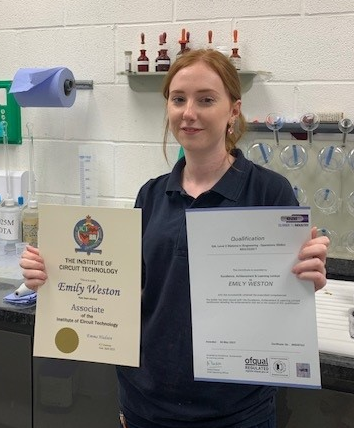
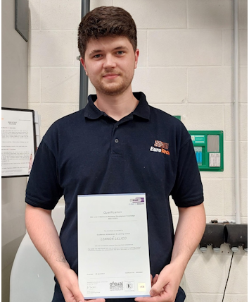
Over the years we have had many young people join us to complete their apprenticeship programmes, most have stayed with us and continued to develop, grow and further their careers. This year’s success stories are Emily Weston and Lennox Lillico.
Read more... |
||
|
|
 PCB007 Editor's Note: The industry lost one of the good ones last weekend when Martin Cotton passed away. Martin not only spent 50 years on the cutting edge of PCB design, he was also, as the axiom goes, "a real character." Everyone who knew Martin has a favorite story about him. At a trade show, Martin once called a group of us younger folks "party poopers" for leaving the bar at 1:30 a.m.; he stayed until 4:30 and still did his presentation at 9 a.m. What else can we say? He was just a hell of a guy. So in honor of Martin and all of the people who loved him, we're publishing this eulogy by EMSNow Publisher Phil Stoten, who knew Martin for over 50 years. Until next time, Martin!
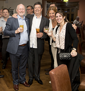 companies including Nortel Networks, Viasystems, Sanmina and Ventec International Group, racking up numerous patents along the way and sharing his intellect and his energy and passion for the industry with trade associations like the ICT (Institute of Circuit Technology) and EIPC (European Institute of Printed Circuits), for whom he spoke on numerous occasions. Less than six months ago, Steve Driver of the ICT presented him with an Honorary Fellowship. Steve Driver said at the time, “Martin has been a huge contributor to the Institute of Circuit Technology for many years. He is a recognised industry expert and is very worthy of this accolade.”
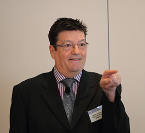 Those that knew Martin as I did, will remember him primarily as the exuberant fun-loving friend that always had your back, and was always up for a big night out, especially if you were lucky enough to spend an evening with him in Munich, after a long day at electronica or productronica. As someone I consider a lifelong friend, that’s how I remember him, but Martin was so much more than just a wonderful friend. I don’t think many would disagree if I said he was a genius and an innovator in his field. When we talked about technology I was always trying to keep up and it seems the entire industry was too. Martin proved it was possible to be too far ahead of the field, and perhaps a little too smart for the rest of the room!

|
Industry News |
|
| Adeon | Wise S.r.l. of Parma, Italy, market leader in horizontal wet machines for PCB manufacturing and chemical mold and contour etching, and Adeon Technologies BV as a member of the CCI Eurolam Group, a leading distributor and industrial service provider for the EMEA electronics manufacturing industry, are proud to announce an expansion of their business relationships. Read more... |
| A-Gas | A-Gas EM are exhibiting at the Nanotexnology 2023 Expo in Thessaloniki Greece. Our very own Alexander Holder will give a presentation on "A Novel Rheological Technique for Characterising Mechanical Properties of UV Curing Materials in Photolithography and Printing Application". Read more... |
| Amphenol - Invotec | Amphenol-Invotec had a successful time exhibiting at at Space-Comm Expo, the UK's largest space event and also The 54th Paris Air Show. Read more... |
| Graphic plc | BAE Global recognises Graphic PLC by awarding them silver status in their 'Partner to Win' programme. This was based on showing high performance levels for both Deliver and Quality, combined with Excellent Customer Service. Read more... |
| Merlin |
In an ever evolving world where the need for sustainable practices is becoming crucial in every business, collaboration between academia and business holds immense potential. The teams at NCAB Group UK Ltd, Merlin PCB Group and Cranfield University are cultivating a mutual understanding of the purpose and objectives of sustainable manufacturing Read more... |
| Pillarhouse | Pillarhouse have launched the AP Master Nozzle. This represents a dramatic leap forward in nozzle performance, offering both improved lifetime and wetting. As these nozzles are now available, you may have questions about how they will fit in with your current soldering platform. Read more... |
| Taiyo | Stuart Down, European Sales Manager from Taiyo America, discusses their growth in European market, partnership with Ventec, and his point of view about the future of European market. Read more... |
| Trackwise | Trackwise have been awarded the prestigious King’s Award for Enterprise for Innovation. Trackwise Designs plc is delighted to be recognised with a prestigious King’s Award for Enterprise. Trackwise has been recognised for its excellence in Innovation Read more... |
| Ventec | Ventec has announced plans to open a new manufacturing facility in Southeast Asia by 2025/26 to extend its manufacturing capabilities beyond China and Taiwan and enhance global supply chain resiliency. Read more... |
| Go back to Contents |
Membership News |
|||||||||||||||||||||||||||||||||||||||||||||||||||||||||||||||||||||||||
|
|
New Members
|
||||||||||||||||||||||||||||||||||||||||||||||||||||||||||||||||||||||||
| Go back to Contents | |||||||||||||||||||||||||||||||||||||||||||||||||||||||||||||||||||||||||
ICT Council Members |
|
|
Council Members |
Emma Hudson (Chair), Andy Cobley (Past Chairman), Steve Payne (Hon Deputy Chairman), Chris Wall (Treasurer), William Wilkie (Technical Director, Hon Sec, Membership & Events), Richard Wood-Roe (Journal Editor & Web Site), Jim Francey, Martin Goosey, Lynn Houghton, Pete Starkey, Francesca Stern and Bob Willis, |
Editors NotesThe ICT Journal |
|
|
Richard Wood-Roe |
Instructions / Hints for Contributors 1. As it is a digital format the length is not an issue. Short is better than none at all! 2. Article can be a paper or a text version of a seminar or company presentation. Please include data tables, graphs, or powerpoint slides. We can shrink them down to about quarter of a page. Obviously not just bullet points to speak from. 3. Photo's are welcome. 4. We would not need source cross references 5. Title of presentation - Of course! Date, Job title of Author and Company represented. 6. An introductory summary of about 150 words would give the reader a flavour of what it's all about. 7. Style - we don't want out and out advertising but we do recognise that the author has a specialism in the product or process that will include some trade promotion. Sometimes it will be a unique process or equipment so trade specific must be allowed. 8. Date and any info relating to where or if this article may have been published before. 9. We can accept virtually any format. Word, Powerpoint, publisher, PDF or Open Office equivalents. 10. Also, to make it easy, the author can provide a word file to go along with his original powerpoint presentation and I/we can merge it together and select the required images. 11. A photo of author or collaborators. I really do look forward to receiving articles for publication. Richard Wood-Roe |